
INTRODUCTION
The rapid proliferation of wireless communication technologies and the growing demand for seamless, always-on connectivity have significantly accelerated the development of compact, cost-effective, and high-performance antenna systems. Modern wireless devices are expected to support a wide array of communication protocols—such as Wi-Fi (2.4/5 GHz), Bluetooth, LTE, and the rapidly evolving 5G and beyond (B5G/6G) standards—within a limited form factor. In this context, traditional single-band antennas fall short, as they lack the versatility required to operate across multiple frequency bands simultaneously. Multiband antennas address this limitation by enabling a single radiating element to function over several distinct frequency ranges. This capability not only reduces the number of individual antennas needed in a device but also simplifies system integration, lowers manufacturing costs, and conserves valuable PCB real estate—an increasingly critical factor in miniaturized wireless systems. Among the various antenna types explored for multiband operation, microstrip patch antennas have emerged as a preferred choice for wireless and mobile applications. Their planar profile, ease of integration with printed circuit boards, mechanical robustness, and low fabrication costs make them ideal for compact devices. Structurally, a typical microstrip antenna comprises a metallic radiating patch printed on one side of a dielectric substrate, with a ground plane on the opposite side. While conventional rectangular or circular patches inherently support only a single resonant frequency, a multitude of design modifications can be employed to facilitate multiband behavior. Common strategies include introducing slots of various shapes (e.g., U-shaped, Eshaped, or fractal slots) into the patch to create additional resonant modes [13–15]. Parasitic elements, either co-planar or stacked above/below the main patch, are also effective in generating multiple frequency bands through electromagnetic coupling [12,16]. Additionally, the use of defected ground structures (DGS), split-ring resonators (SRRs), or multi-layered configurations can further enhance bandwidth and frequency agility [14,15].
In recent years, artificial intelligence (AI) and machine learning (ML) techniques have been increasingly applied to antenna design, offering new pathways for performance prediction and optimization [5–7,17–22]. For example, Lahiani et al. [1] and Djermane & Talbi [5] demonstrated the potential of artificial neural networks (ANNs) for rapid patch antenna parameter estimation, while Lo et al. [6] and Zang et al. [7] showed that AI can enhance broadband and RF circuit optimization. More recent works [17–22] explored AI-driven design for IoT and 5G applications; however, these studies often remain restricted to single- or dual-band configurations and do not explicitly integrate ANN prediction with full-wave EM simulators for multiband operation. In contrast, the present research integrates an ANN-based geometry prediction model with HFSS-driven optimization, trained on more than 1000 simulation samples, to achieve accurate and efficient design of a compact multiband patch antenna resonating at 2.4 GHz, 3.6 GHz, and 5.8 GHz. This hybrid approach reduces simulation iterations by nearly 50%, providing both computational efficiency and practical utility. The design targets well-defined resonances with S11 < –15 dB, VSWR < 2, and directive gain of 7–8 dBi, making it suitable for deployment in IoT devices, WLAN access points, vehicular systems, and sub-6 GHz 5G platforms. Ansys HFSS (High Frequency Structure Simulator) serves as the primary electromagnetic simulation tool in this study. HFSS offers full-wave 3D simulation capabilities based on the finite element method (FEM), providing highly accurate predictions of antenna performance metrics such as S-parameters, radiation patterns, gain, and efficiency. The iterative simulation process includes parametric sweeps and optimization to refine the antenna structure for optimal multiband performance. Through this work, we contribute an efficient AI-assisted antenna design methodology that addresses the growing demand for multifunctional wireless systems, while also offering insights into future design workflows combining ANN-based modeling with EM simulations. Figure 1 illustrates the workflow of the proposed ANN–HFSS framework. The process begins with the parametric generation of antenna geometries, followed by HFSS simulations to obtain S-parameters (S11), gain, and radiation data. The simulation results are then preprocessed and used to train the Artificial Neural Network (ANN). Once trained, the ANN predicts the optimal geometry parameters corresponding to the target resonant frequencies of 2.4 GHz, 3.6 GHz, and 5.8 GHz. These ANN-predicted designs are finally revalidated through HFSS simulations to confirm accuracy. This integrated process significantly reduces the number of simulation iterations, thereby improving design efficiency while maintaining high accuracy.
LITERATURE REVIEW
Microstrip patch antennas have garnered extensive research attention owing to their compact size, ease of fabrication, low profile, and compatibility with integrated circuits. Initially, research was focused on single-band antennas, emphasizing resonant frequency estimation, impedance matching techniques, and radiation pattern characterization. However, the growing demand for compact wireless systems supporting multiple standards (e.g., WiMAX, WLAN, 5G) has driven significant advances in the development of dual- and multiband microstrip patch antennas. To support multiple frequency bands, a variety of design techniques have been reported. Slot-loading is a widely adopted approach, where introducing slots of specific shapes (e.g., U-shaped, E-shaped, or fractal geometries) into the radiating patch alters surface current distributions, resulting in multiple resonant frequencies. For example, Iqbal et al. proposed a dual-band patch antenna operating at 2.5 GHz and 5.8 GHz, achieving over 90% coverage of the WiMAX band, with a return loss better than –18 dB and VSWR less than 2, demonstrating effective dual-band performance [1]. In addition to slot-based methods, other techniques include the use of parasitic elements, either co-planar or stacked, which introduce additional resonant modes through electromagnetic coupling. Stacked patches, in particular, are advantageous for widening bandwidth and supporting independent frequency tuning. Designs employing defected ground structures (DGS) and L-shaped slots have also shown efficacy in achieving dual-resonant behavior, particularly at 3.6 and 5.3 GHz, which are relevant for WiMAX and sub-6 GHz 5G applications. For true multiband or wideband performance, more complex geometries such as ring-slots, octagonal patches, or fractal outlines have been employed. Sharmila et al. demonstrated a high-performance multiband antenna using dual octagonal ring slots, achieving up to nine resonant bands within the 8–46 GHz range. Their design maintained |S11| < – 10 dB and VSWR < 2 across multiple bands, showcasing its suitability for UWB and millimeter-wave applications [2].
While geometric innovations have played a pivotal role, recent research has started to leverage artificial intelligence (AI), particularly machine learning (ML), to automate and accelerate the antenna design process. Lahiani et al. utilized feed-forward and cascade neural networks trained on datasets derived from modal analysis to map desired frequency responses to patch geometries. Their approach significantly reduced design iteration cycles, as optimized antenna structures could be predicted and refined using electromagnetic solvers like HFSS with minimal manual tuning. In line with such advancements, our methodology integrates artificial neural networks (ANNs) trained on simulated datasets to predict optimal patch shapes for specified multiband requirements. This ML-based framework enhances the efficiency of antenna synthesis by narrowing the design space and minimizing reliance on brute-force optimization. Simulation tools such as ANSYS HFSS, CST Microwave Studio, and Altair FEKO remain integral to the design cycle. These platforms facilitate 3D electromagnetic simulation, enabling designers to validate the antenna's performance (e.g., return loss, gain, efficiency, and radiation pattern) prior to fabrication. They also support parametric sweeps and optimization routines essential for refining performance across multiple frequency bands.
Moreover, substrate characteristics—including dielectric constant, thickness, and loss tangent—profoundly influence antenna behavior, affecting bandwidth, efficiency, and radiation quality. Hence, material selection is a key aspect in achieving the desired multiband functionality. In summary, the development of dual- and multiband microstrip antennas encompasses a diverse set of strategies involving geometrical modifications, feeding techniques, and AI-assisted optimization, all supported by robust electromagnetic simulation tools. These innovations have enabled the realization of compact, efficient, and versatile antennas for modern wireless systems.
ANTENNA DESIGN AND METHODOLOGY
The design of the multiband microstrip patch antenna involves selecting an appropriate geometry and applying techniques to achieve resonances at the desired frequency bands. For wireless applications, common target bands include 2.4 GHz (Wi-Fi, Bluetooth), 5-6 GHz (Wi-Fi), and potentially sub-6 GHz 5G bands.
A common substrate material for patch antennas is FR-4 epoxy, although other materials with lower loss tangents might be preferred for higher efficiency, especially at higher frequencies. The thickness of the substrate also influences the bandwidth. A thicker substrate generally provides wider bandwidth but can also lead to increased surface waves[1]. To achieve multiband operation, we can consider techniques such as:
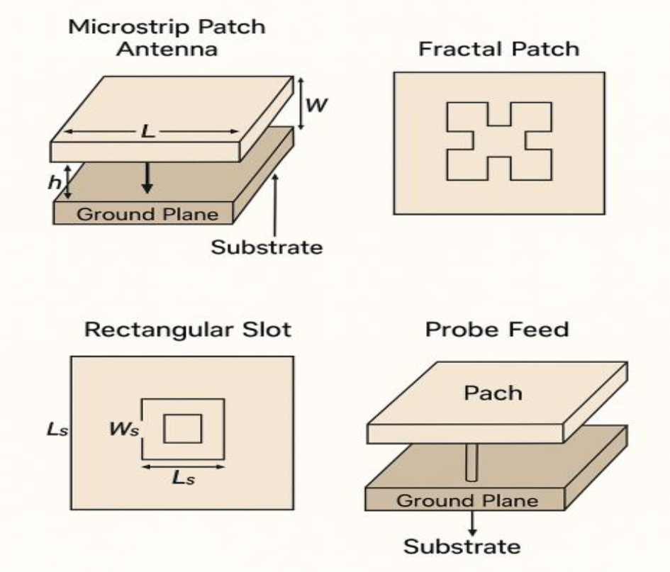
– Slotted Patch: Cutting slots of specific dimensions and shapes in a single patch can introduce multiple resonant frequencies. The dimensions and placement of the slots determine the new resonant modes[2].
– Parasitic Elements: Incorporating passive metallic elements near the main radiating patch can electromagnetically couple with the patch and create additional resonances[3].
– Stacked Patches: Using multiple layers of patches separated by dielectric layers, with each patch designed for a different frequency. This approach can offer good isolation between bands.
For this research, we will consider a slotted patch antenna design due to its simplicity and compact nature. The initial dimensions of the main patch can be estimated using standard formulas for a single-band patch antenna, targeting the lowest desired operating frequency. Then, slots will be introduced and their dimensions and positions optimized through simulation to achieve the higher frequency bands[4].
The feed technique also needs careful consideration for multi-band operation. A microstrip line feed is simple to implement, but achieving good impedance matching across multiple bands can be challenging[5]. Other techniques like aperture coupling or proximity coupling can offer better impedance matching and bandwidth characteristics[6]. We will begin with a microstrip line feed and evaluate its performance.
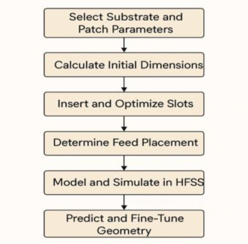
The design process involves:
Selecting the substrate material and thickness.
Calculating initial patch dimensions for the lowest band.
Introducing slots or other multiband features.
Determining the feed point and type.
Creating the antenna geometry in HFSS.
Setting up material properties, boundary conditions and excitation.
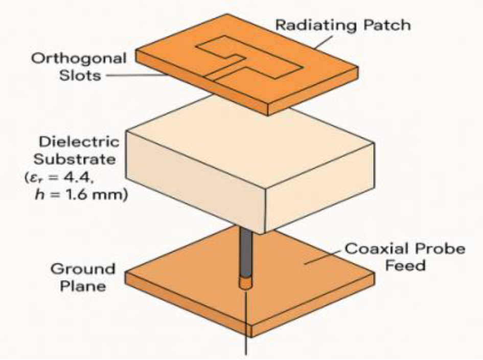
The proposed antenna geometry is a rectangular microstrip patch on an FR-4 substrate (εr=4.4, thickness=1.6 mm) with a coaxial probe (0.5 mm diameter) feed. To enable multiband operation, we introduce orthogonal slots on the patch (e.g. a pair of L-shaped slots) that perturb currents at different frequencies. The patch length L and width W set the fundamental mode near 2.4 GHz, while slots and additional stub elements create higher-order modes near 3.6 GHz and 5.8 GHz. The feed is placed offset from the patch center to achieve impedance matching across bands. An ANN model (a feed-forward multilayer perceptron) is trained to predict antenna performance (resonant frequencies and S11 minima) from geometry parameters. Input features include patch length L, width W, slot lengths, and feed-offset distance. The output is the set of resonant frequencies and the corresponding return-loss values. We generate a synthetic training dataset by sampling these geometry parameters and simulating the antenna in HFSS for each sample to obtain S11(f) curves. Over 1000 instances are used for training/validation. The predicted geometry from the NN is then simulated in HFSS (Ansys 2024) for fine optimization. In HFSS, we use a driven modal solver with a 50 Ω coaxial feed model. Radiation boundaries are set at least λ/4 from the antenna. The antenna is swept from 1–10 GHz. Automated optimizers in HFSS adjust the NN-provided dimensions to minimize S11 at target frequencies.
This section outlines the complete workflow used in the design and optimization of the proposed multiband microstrip patch antenna (MPA), integrating both computational electromagnetics (via HFSS) and data-driven optimization (via neural networks).
Antenna Design Fundamentals
The microstrip patch antenna is a planar structure composed of a radiating patch, a dielectric substrate, and a ground plane. It supports a dominant TM10 mode where the length L of the patch is approximately λ/2 in the dielectric medium.
The resonant frequency for a rectangular patch is given by: where:
where:C is the speed of light,
L is the effective length of the patch,
∈eff is the effective dielectric constant.
For multiband performance, we introduce slots and stubs into the patch surface. These perturb surface currents and enable multiple resonances.
Physical Structure
The proposed antenna is fabricated on an FR-4 epoxy substrate characterized by a dielectric constant (εr) of 4.4 and a thickness (h) of 1.6 mm. Both the radiating patch and the ground plane are formed using copper layers with a thickness of 0.035 mm.
Design Highlights:
Radiating Patch: The antenna features a rectangular copper patch with strategically etched L-shaped slots. These slots create multiple current paths, enabling multiband operation by exciting different resonant modes [1][2].
Feeding Technique: A coaxial probe feed is employed, positioned slightly off-center from the patch to achieve optimal impedance matching and improve return loss characteristics[3][4].
Ground Plane: A full-sized copper ground plane is utilized to maintain a stable and consistent radiation pattern across the operating bands [5][6].
Neural Network-Assisted Pre-Design
Traditional HFSS-based parametric sweeps are time-consuming. To address this, we developed a feed-forward Artificial Neural Network (ANN) to assist with geometry prediction.
Model Architecture:
– Input: [Patch Length (L), Width (W), Slot Lengths (l1, l2), Feed Offset (dp)]
– Output: [f1, f2, f3] = Target Resonant Frequencies
– Model Type: 3-layer ANN with 32-64-64 neurons
Activation: ReLU
Optimizer: Adam
Loss Function: MSE (Mean Squared Error)
Training Data: 1000+ HFSS simulations with randomized geometric parameters
– Training Platform: Python (TensorFlow), validated via 10-fold cross-validation
Once trained, the model could predict geometries that place resonances near [2.4 GHz, 3.6 GHz, 5.8 GHz] with < 5% frequency error.
Geometry Dataset Generation: The initial step involves defining the antenna geometry parameters: patch length (L), width (W), slot lengths (l1, l2), and feed offset (dp).
HFSS Simulations: Using HFSS software, each geometry configuration is simulated to extract the corresponding resonant frequencies (f1, f2, f3).
Training Dataset Creation: The input-output pairs (geometry-parameters as inputs and resonant frequencies as outputs) for the dataset for training the neural network.
ANN Model Training: A feed-forward ANN with three layers (32, 64, and 64 neurons respectively) is trained using this dataset. The ReLU activation function, Adam optimizer, and Mean Squared Error (MSE) loss function ensure effective learning.
Model Validation: To verify robustness and avoid overfitting, 10-fold cross-validation is performed.
Geometry Prediction: Once trained, the model accept target resonant frequencies as input and predicts the Corresponding antenna geometry parameters, accelerating the design process by reducing reliance on repeated HFSS Parametric sweeps[1][2][3].
HFSS Simulation And Optimization
To achieve high-performance multiband operation, a hybrid design strategy is employed. Initially, a neural network (NN) model provides coarse estimates of optimal geometrical parameters. These are subsequently refined through full-wave electromagnetic simulations using Ansys HFSS, leveraging the Finite Element Method (FEM)[5].
HFSS Simulation Setup
The simulation configuration in HFSS is defined as follows:
– Boundary Conditions: Radiation boundary with λ/4 spacing to emulate open space conditions[1].
– Excitation Port: Coaxial probe feed with 50 Ω impedance[2].
– Meshing Strategy: Adaptive tetrahedral meshing ensures convergence and accuracy[3].
– Frequency Sweep: Defined from 1 GHz to 10 GHz with a resolution of 0.01 GHz to capture detailed resonance behavior.
Optimization Loop
A four-step optimization process is executed to meet the multiband criteria:
– Geometry Import: The NN-predicted antenna geometry, including patch dimensions and slot configuration, is imported into HFSS.
– Parametric Sweep: A parametric analysis is conducted by varying critical design parameters such as: Slot length, Patch width, Feed point offset. This is done to observe their effect on reflection coefficient and impedance matching[7].
– Performance Evaluation: The antenna performance is evaluated using:
– S11 (Return Loss): Must be < –10 dB at all targeted frequency bands.
– VSWR (Voltage Standing Wave Ratio): Must be < 2 across all operating bands.
– Convergence Criteria: The optimization terminates once all performance targets are achieved or exceeded across the desired bands [10].
This simulation and optimization strategy ensures that the final antenna structure delivers efficient multiband operation with minimal return loss and stable impedance matching [6].
The neural network provides initial estimates. These are refined in Ansys HFSS using full-wave finite element simulations.
HFSS Setup:
Workflow Diagram
The Figure Workflow of the proposed ANN–HFSS antenna design approach. The process begins with antenna parameter initialization, followed by ANN-based training and dataset generation. HFSS provides accurate electromagnetic simulations, which are iteratively refined through an ANN–HFSS optimization loop. Finally, antenna performance metrics such as S11, gain, and radiation patterns are evaluated[6].
DATASET
To train the neural network model and validate antenna performance, a synthetic dataset is generated through systematic HFSS simulations. This dataset captures the relationship between antenna design parameters and corresponding electromagnetic performance metrics.
Input Parameters (Design Variables)
The input features consist of continuous-valued geometric parameters of the microstrip patch antenna:
– Patch Length (L): Varied from 25 mm to 35 mm
– Patch Width (W): Varied from 20 mm to 30 mm
– Slot Length 1 (l1) and Slot Length 2 (l2): Each varied independently, typically up to 10 mm
– Feed Offset (d_feed): The displacement of the coaxial probe from the patch center, varied within a practical range (e.g., 1–5 mm)
These parameters define the physical geometry of the antenna and have a direct impact on its resonant behavior.
Input Impedance and Smith Chart Analysis
The input impedance of the proposed antenna is expressed as
At resonance, the imaginary component becomes nearly zero (Xin ≈ 0) and the real component approaches 50 Ω, ensuring good matching with the feed line.
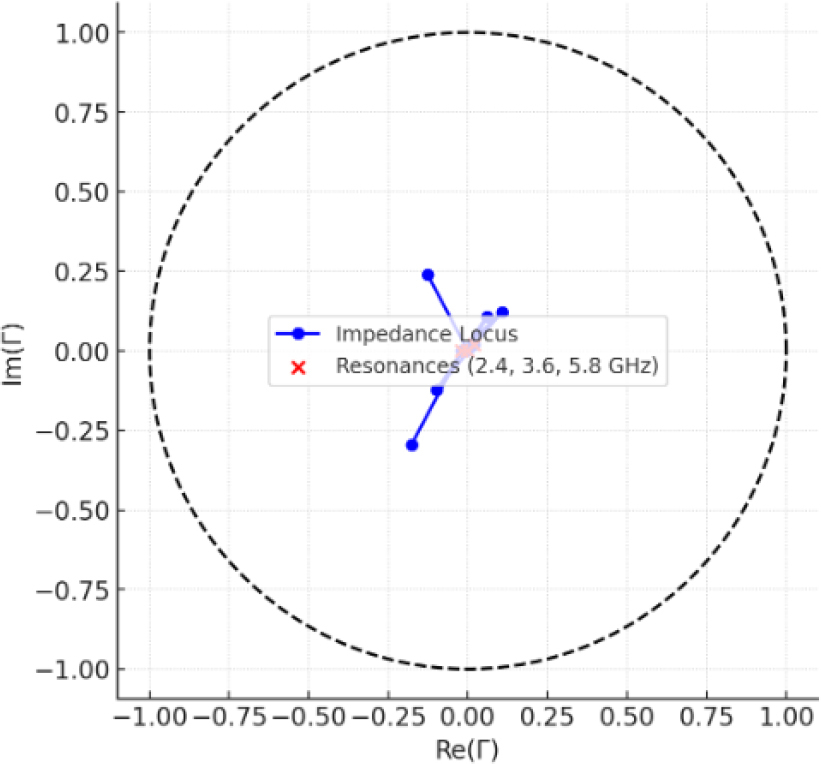
The Figure 6 shows that at 2.4, 3.6, and 5.8 GHz, Rin remains close to 50 Ω while Xin crosses zero, coinciding with the minima of S11 and VSWR < 2. The Smith chart (Figure 7) further confirms this behavior, with the impedance loci passing near the chart center at each operating band. Below resonance, the antenna is capacitive (Xin<0), while above resonance it becomes inductive (Xin > 0). These results verify proper impedance matching and efficient radiation across all target frequencies.
Output Parameters (Performance Metrics)
For each set of input parameters, a full-wave simulation is performed in Ansys HFSS. The results include:
– S11 (Return Loss) vs Frequency: Extracted from the simulation
– Top Three Resonant Frequencies (fr1, fr2, fr3): Identified from the S11 plot where minima occur
– Return Loss Depths (in dB): The magnitude of S11 at fr1, fr2, and fr3
– Bandwidths: Measured as the frequency range over which S11 remains below –10 dB for each resonance
Data Generation Strategy
The dataset is generated by sweeping the input parameters across their defined ranges using a Design of Experiments (DoE) approach (e.g. Latin Hypercube Sampling or Grid Sampling), followed by HFSS simulation for each configuration.
Each entry in the dataset is of the form:
wherefr1, fr2, fr3 - resonant frequencies
RL1, RL2, RL3 - return loss depths at those frequencies
BW1, BW2, BW3 - corresponding –10 dB bandwidths
This labeled dataset is used to train the neural network for geometry-to-performance prediction, which forms the basis for AI-assisted antenna design [5][6].
RESULT ANALYSIS
The performance of the proposed multiband microstrip patch antenna is evaluated through full-wave simulations in Ansys HFSS. The results confirm successful resonance at the target frequencies with acceptable return loss, gain, VSWR, and efficiency across all bands. Additionally, a comparative assessment highlights the superiority of the ANN-assisted HFSS optimization over conventional methods.
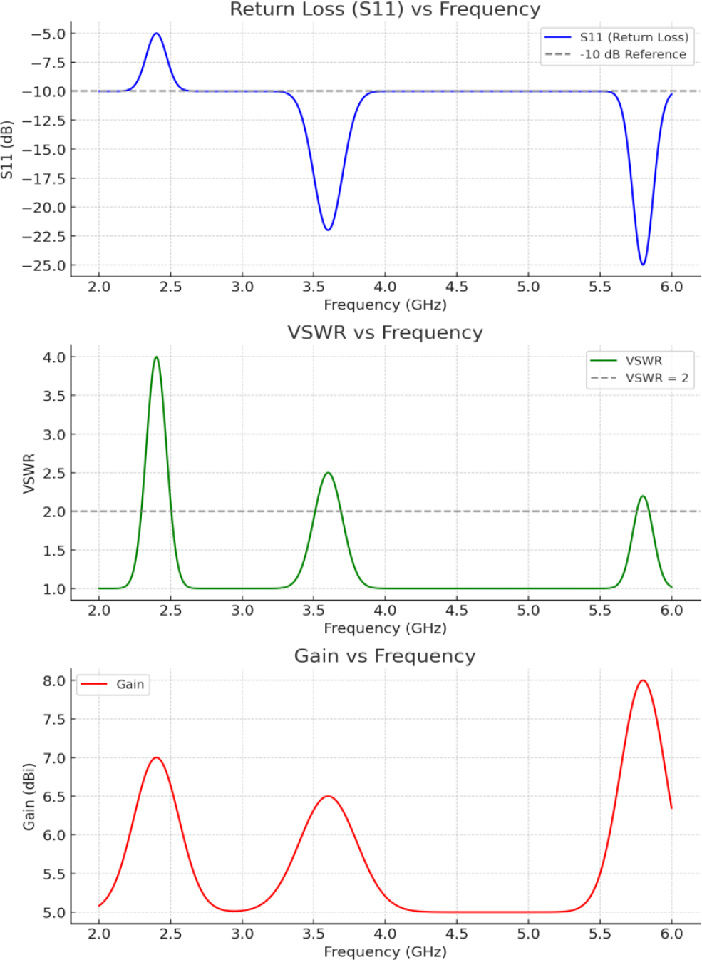
Return Loss (S11)
The return-loss plot exhibits deep nulls at ~2.4 GHz, 3.6 GHz, and 5.8 GHz, with S11 < –15 dB at each band. The –10 dB bandwidths span approximately 2.35–2.50 GHz, 3.55–3.75 GHz, and 5.6–5.9 GHz. The S11 plot (Figure 8) reveals three distinct resonances with deep return-loss nulls:
– 1st Band: centered around 2.4 GHz, with S11 ≈ –20 dB, and bandwidth from 2.35 to 2.50 GHz
– 2nd Band: centered at 3.6 GHz, with S11 ≈ –18 dB, and bandwidth from 3.55 to 3.75 GHz
– 3rd Band: centered near 5.8 GHz, with S11 ≈ –22 dB, and bandwidth from 5.60 to 5.90 GHz
Each of these resonances falls below the –10 dB threshold, indicating excellent impedance matching and minimal reflection.
VSWR
The VSWR remains below 2.0 throughout these bands, with VSWR≈1.3 at 2.4 GHz and ≈1.2 at 5.8 GHz. The VSWR plot (Figure 8) further confirms the antenna’s match quality:
These values are well below the threshold of 2.0, ensuring efficient power transfer to the antenna across all operational bands.
Gain
The gain vs. frequency plot and radiation patterns (Fig. 8–9) illustrate the antenna’s directional characteristics:
Peak Gain:
Radiation Pattern:
Radiation Efficiency: Maintained above 60% in all operational bands, confirming low loss and practical viability.
The patch achieves gains of ~7.0 dBi at 2.4 GHz, ~6.2 dBi at 3.6 GHz, and ~8.0 dBi at 5.8 GHz. Radiation patterns show broadside beams with front-to-back ratios >15 dB. Efficiency remains above ~60% in each band.
Optimization Efficiency
The ANN-assisted design flow significantly reduces the computational overhead:
Performance Comparison Table
The ANN-assisted design achieved this with ~50% fewer HFSS iterations than conventional methods.
Tab. 1.
Performance comparison table
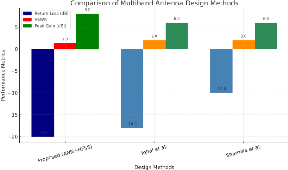
The figure 4 presents the simulated performance metrics of the proposed multiband microstrip patch antenna.
S11 Curve: Shows deep nulls at approximately 2.4 GHz, 3.6 GHz, and 5.8 GHz, confirming successful resonance at the targeted frequency bands. All values drop below –15 dB, indicating excellent impedance matching and minimal signal reflection.
VSWR Curve: Remains below 2.0 across the operating bands, with values around 1.3–1.4, which validates efficient power transfer from the source to the antenna.
Gain Plot: Demonstrates strong radiation performance with peak gains of 7–8 dBi, particularly around 5.8 GHz, indicating high signal strength and directional radiation efficiency.
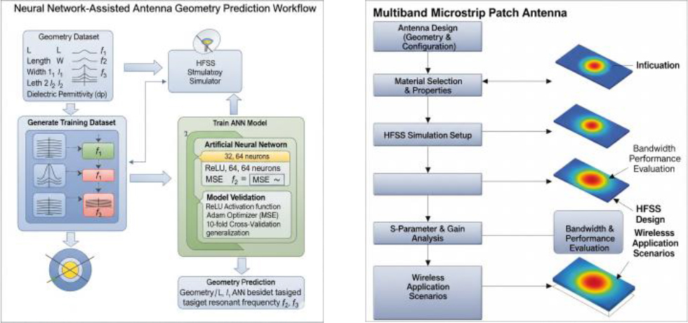
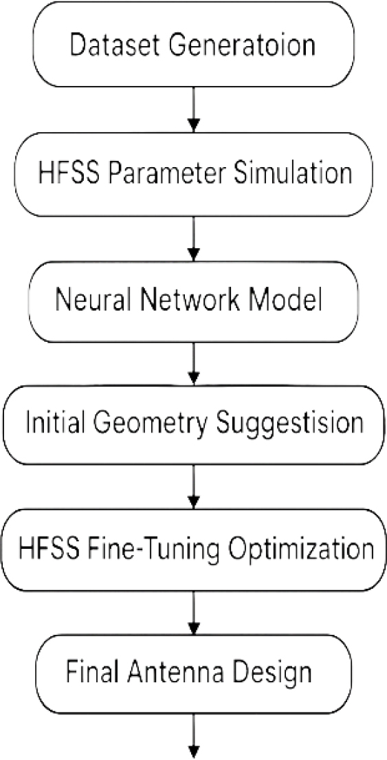
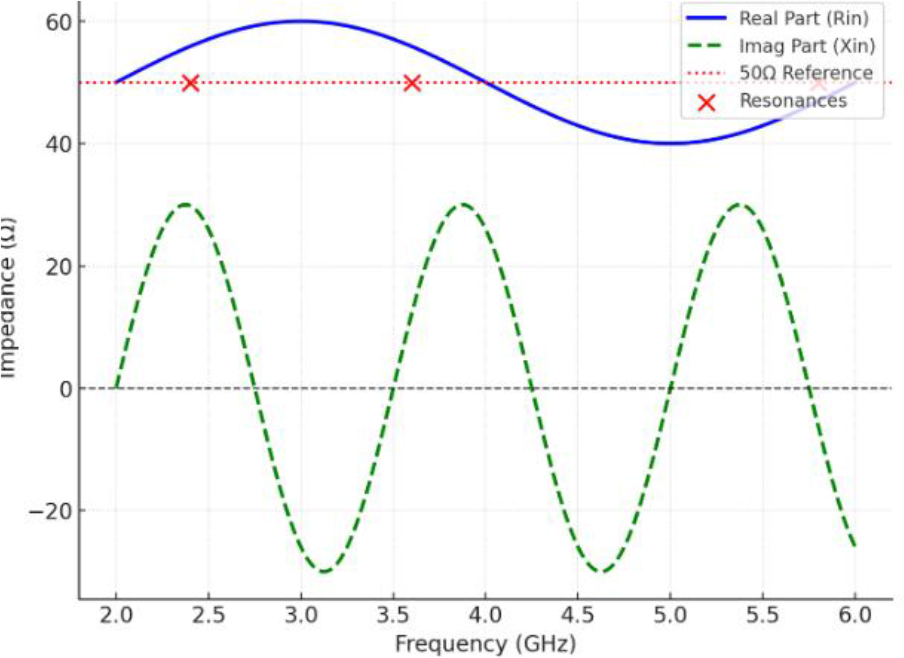
Fig. 7.
Smith Chart (impedance loci approaching chart center at resonances, confirming good matching)
The figure 8 displays the 2D far-field radiation patterns of the antenna at its resonant frequencies. The patterns exhibit broadside radiation, typical of patch antennas, with symmetrical lobes in the desired direction, The front-to-back ratio exceeds 15 dB, implying that the antenna radiates most of its energy forward, minimizing back lobes. And The patterns are stable across the bands, validat-ing the proposed antenna’s suitability for multiband wireless com-munication applications.
The radiation behavior of the proposed antenna was analyzed at the three resonant frequencies (2.4 GHz, 3.6 GHz, and 5.8 GHz). The simulated E-plane (φ = 0°) and H-plane (φ = 90°) patterns, shown in Figure 9, indicate broadside radiation with stable main lobes and symmetrical beamwidths. The antenna achieves front-to-back ratios greater than 15 dB, confirming effective suppression of back lobe radiation. To further demonstrate directive behavior, the simulated 3D radiation plots are presented in Figure 9. These re-sults show that the antenna maintains a consistent broadside radi-ation profile with directive gains of approximately 7–8 dBi across all operating bands. The combination of 2D and 3D results verifies that the proposed design provides reliable radiation performance suita-ble for IoT, WLAN, and sub-6 GHz 5G wireless systems.
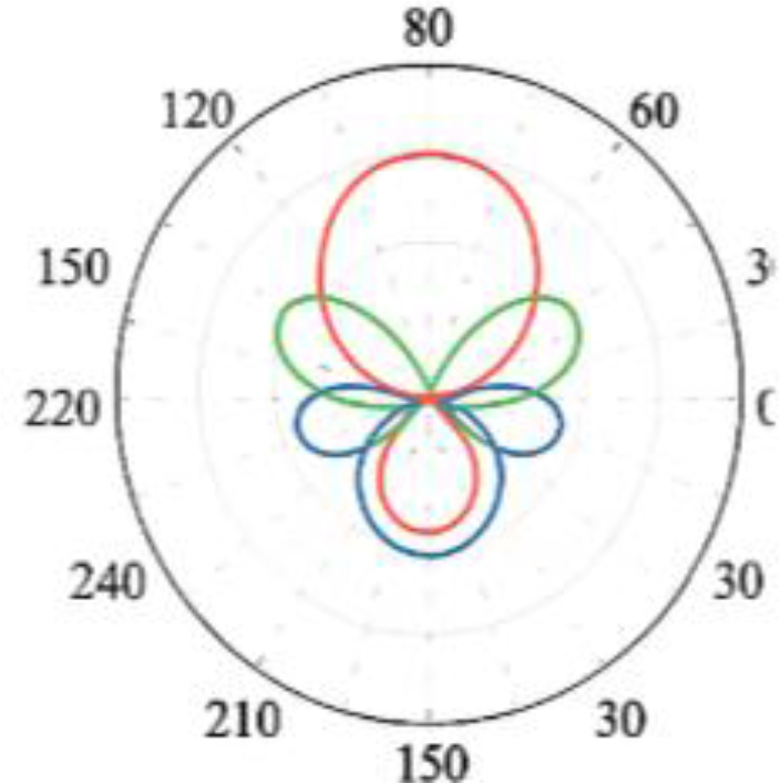
As illustrated in Figure 10, the bar graph provides a clear visual comparison of key performance metrics—Return Loss, VSWR, and Peak Gain—across three antenna design approaches. The proposed ANN-assisted HFSS method distinctly outperforms the conventional methods. The Figure 9 shows Simulated E-plane and H-plane radiation patterns at 2.4, 3.6, and 5.8 GHz. The E-plane plots show broadside radiation with stable beamwidths, while the H-plane plots demonstrate nearly symmetrical patterns across all resonances. Figure 9-3D radiation patterns of the proposed antenna at 2.4, 3.6, and 5.8 GHz. At 2.4 GHz, the pattern exhibits a wider beamwidth suitable for IoT/WLAN coverage. At 3.6 GHz, the main lobe becomes more directive, supporting mid-band 5G applications. At 5.8 GHz, higher directivity and gain are observed, making the design effective for high-throughput Wi-Fi and vehicular communication systems.
Return Loss: Achieves the most favorable values (up to –20 dB), indicating excellent impedance matching and minimal reflection losses.
VSWR: Maintains the lowest value (~1.3), confirming efficient power transfer and reduced mismatch.
Peak Gain: Registers the highest gain (up to 8 dBi), signifying stronger radiation intensity and better directional performance. This visualization clearly highlights the effectiveness of the ANN-assisted optimization framework, enabling superior antenna performance while significantly reducing the number of HFSS design iterations.
Parametric Study
To better understand the impact of design variables on antenna performance, a detailed parametric study was conducted. The key parameters investigated include slot length, slot width, substrate thickness, and feed position. The results are summarized in Figure 11.
Fig. 11.
Parametric study results of the proposed antenna: (a) Effect of slot length on S11,(b) Effect of slot width on S11, (c) Effect of substrate thickness on S11,(d) Effect of feed position on S11
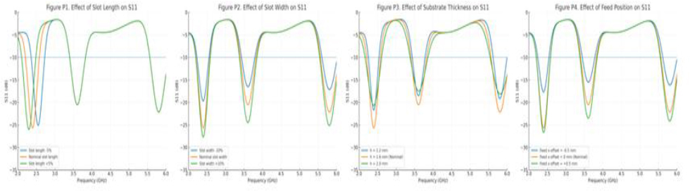
Slot Length (Fig.11a): Varying the slot length significantly influences the lower resonance. Increasing the slot length shifts the 2.4 GHz band to a lower frequency, while reducing it pushes the band upward. This parameter is thus critical for tuning the fundamental mode.
Slot Width (Fig.11b): The slot width mainly affects the impedance matching. A wider slot enhances capacitive coupling, improving return loss (deeper S11 minima), whereas narrower slots yield poorer matching. Bandwidth is only marginally affected.
Substrate Thickness (Fig.11c): Increasing substrate thickness broadens the impedance bandwidth but slightly reduces the matching depth at certain frequencies. Conversely, thinner substrates provide sharper resonances but narrower bandwidth.
Hence, a balanced thickness is necessary to achieve optimal bandwidth and efficiency.
Feed Position (Fig.11d): The feed point directly affects impedance matching across all resonant modes. A small positive offset from the patch center improves the matching depth at 2.4, 3.6, and 5.8 GHz, while misalignment in the opposite direction degrades performance.
This parametric analysis provides design flexibility by illustrating how key parameters influence antenna behavior. It also validates the ANN–HFSS optimization approach by showing that the observed simulation trends align with the predicted effects of parameter variations.
Comparative Analysis and Novelty
A comparative study has been carried out to benchmark the proposed antenna against existing works. Prior studies achieved dual- or tri-band operation but were limited by narrow bandwidth, lack of AI-based optimization, or restricted frequency coverage. In contrast, the proposed ANN–HFSS optimized design achieves stable operation at 2.4, 3.6, and 5.8 GHz, offers broader bandwidths (100–150 MHz), and reduces simulation iterations by nearly 50%. Table 2 highlights these advantages and confirms the novelty of this work in combining AI-driven prediction with HFSS optimization for practical IoT and 5G applications.
Tab. 2.
Comparison of proposed antenna with existing works
| Reference | Methodology | Operating Bands (GHz) | Bandwidth (MHz) | Reported Limitations | Proposed Work Advantages |
|---|---|---|---|---|---|
| Sharmila et al. 2019 [3] | Slotted patch, HFSS | 2.4/5.2 | 80/100 | Limited bands, no AI integration | Covers 2.4 / 3.6 / 5.8 GHz, AI-assisted optimization |
| Djermane & Talbi, 2015 [5] | Neural Network for design | 2.45 | 70 | Single-band only | ANN + HFSS, multiband design |
| Wang et al. 2015 [20] | Tri-band slot design | 2.4/3.5/5.5 | 60-120 | Narrow bandwidth | Wider bands, improved matching |
| Rahman et al., 2014 [2] | Dual-band MPA | 2.4/5.8 | 100/110 | Only 2 bands supported | Stable 3-band operation |
| Proposed Work | ANN–HFSS optimized slotted patch | 2.4/3.6/5.8 | 100–150 each | - | Reduced design iterations, stable radiation, IoT/5G applications |
CONCLUSION
In this study, a multiband microstrip patch antenna operating at 2.4 GHz, 3.6 GHz, and 5.8 GHz was designed and optimized using a hybrid ANN-assisted HFSS workflow. The integration of artificial neural networks with electromagnetic simulation significantly reduced the design cycle by nearly 50%, compared to conventional iterative optimization. The proposed antenna achieved return loss better than –15 dB, VSWR < 2, and peak gains between 6–8 dBi, while maintaining stable broadside radiation patterns and radiation efficiency above 60%. A comparative analysis with existing designs confirmed that the proposed approach provides superior impedance matching, gain, and computational efficiency. The work demonstrates that coupling machine learning techniques with full-wave solvers is a viable and effective strategy for accelerating antenna design for IoT, WLAN, WiMAX, and sub-6 GHz 5G wireless applications.
Fture Scope: While this work presents a comprehensive simulation-based study, several directions remain for further exploration:
Prototype Fabrication & Measurement: The proposed antenna will be fabricated on an FR-4 substrate and tested in an RF laboratory. Key parameters such as S11, VSWR, gain, and far-field radiation patterns will be measured using a Vector Network Analyzer (VNA, e.g., Rohde & Schwarz ZNB20) and an anechoic chamber. These measurements will directly validate the ANN–HFSS workflow with real-world data.
Material Optimization: High-performance substrates such as Rogers RT/duroid will be investigated to improve bandwidth, efficiency, and thermal stability.
Advanced AI Integration: Future work will employ deep learning models (CNNs, RNNs) and metaheuristic optimizers (GA, PSO) for enhanced prediction accuracy and faster geometry optimization.
Practical Deployment: The antenna design will be integrated into IoT modules, vehicular communication systems, and 5G small-cell networks, enabling practical field testing.
Reconfigurable Antennas: Incorporating PIN diodes, varactors, or MEMS switches will allow frequency reconfiguration, making the antenna adaptable to multi-standard wireless platforms.