
Introduction
In recent years, significant developments occur in the additive manufacturing industry, due to the entry barriers such as the price of machinery and materials decreasing, the appearance of an increasing amount of literature helpful to understanding the process, and technological developments enabling to manufacture of more precise instruments.
The precision is a factor visible especially in photo-curing additive manufacturing techniques, where the pre-product – a polymeric resin or a composite in a liquid form is cured layer-by-layer, via 3 different methods – Stereolithography (SLA), Digital light processing (DLP) or liquid-crystal display photo-curing (LCD or MSLA – masked stereolithography). Those techniques differ from each other in the method of exposing layers of material to UV (ultraviolet) light. In the first case layer patterns are obtained by utilization of a focused laser, in the second case projector generates the light pattern, and in the latter – an LCD screen is used to mask the light generated by a UV lamp in selected areas to cure the resin.
LCD printing sees significant development currently, in terms of the display quality and resolution increasing, as well as market growth due to its extension to household applications. The resolution possible to obtain with low-cost machines is best quantified by single pixel size. Currently the machines can achieve pixel dimensions within a range between 18 [1] and 25 µm [2, 3], making those suitable for applications in microdevices manufacturing. DLP 3D printers designed for micromanufacturing can achieve pixel resolution as small as 5 µm [4].
Development in material science and applied 3D printing is also visible in modern literature. A good example of that would be development of phosphorescent and photoluminescent materials for sensor design and optical data storage [5] along with new display methods [6]. Tunable afterglow effect developed and described in [7] for 3D printable material can also be used for structural monitoring, and is, in that case, achieved by manipulating photocuring time and process humidity. By manipulating DLP process parameters, namely by varying the curing light intensity, different cross-linking effects can be achieved, leading to lower molecular weight of the product, end different electrical resistance, enabling the development of new 3D printed functional electronic devices [8]. Phosphorescence of modern 3D printed materials can also be achieved by doping a polymer matrix, allowing creation of self-monitoring microfluidic chips [9].
Microdevices and their manufacturing methods grow in importance in fields such as sensors, surveillance devices and semiconductors [10], biology and chemistry [11], to name a few. Among those, microfluidic devices (MD), are a group of microdevices with a variety of novel applications in chemistry, biology and medicine [12], ranging from testing equipment to precise drug distribution systems [13–16], microdosing and micropipetting [17], biosensors for biomarkers detection [18], micropumps and valves [19, 20], wearable structures such as actuators, sensors and optical components [21].
Microfluidic devices can be manufactured with a range of methods, depending on the device’s material, required dimensions, and structural shape. Currently, the most precise MF devices can be manufactured with laser etching on glass with an accuracy of around 1 µm, however, manufacturing with such a method is limited by the debris generated during manufacturing, especially with long thin channels. Manufacturing methods of MF devices can be assigned to groups: micromachining, soft lithography, in situ construction and micromolding [22]. The cost of prototyping and manufacturing MF devices, as well as lack of standardization are limiting factors in MF development [12].
Additive manufacturing is often mentioned as one of the methods allowing to obtain MF devices by either FDM (fused deposition modelling) [23–26] or DLP methods [27]. FDM is mainly used to form sacrificial molds, so the manufacturing method is complex and indirect. According to [27] DLP is a method with which a resolution of 10 µm can be achieved, but the method is not cost-effective. In [28] a 3D biomimetic structure for microdroplet manipulation was presented, manufactured with DLP, with the main dimensions of a singular structure being 40 and 100 µm. Different structure for droplet microfluidics was presented in [29], specifically converging structures and microwells utilized for storing droplets to ease observations. Authors in [29] state that 3D printing can be used instead of soft lithography to manufacture such devices, but their precision is lower in comparison. Different trapping structures are described in [30], with the smallest dimension being 100 µm, which makes LCD printing a suitable method of manufacturing for them. More complex microwell trapping structures with a diameter of 60 µm can also be manufactured using PHASR (photoactivated selective release) fabrication protocol [31]. Complete biomimetic devices – artificial cells for vesicle production with dimensions ranging between 10 and 130 µm can also be manufactured [32]. Liquid glass additive manufacturing is also possible in the MF domain but with an accuracy (smallest dimensions of structures) of 200 µm [33].
The current literature lacks precise information for researchers about the issues they might encounter as well as results they might expect while selecting photo-curing LCD printing as a method for manufacturing specific microdevices, with most of the literature focusing on DLP techniques. Therefore, in this article, various patterns suitable for casting PDMS microfluidic 2D devices, manufactured via photo-curing LCD printing, were designed, and examined in terms of dimensional accuracy and shape reproducibility.
Methods And Materials
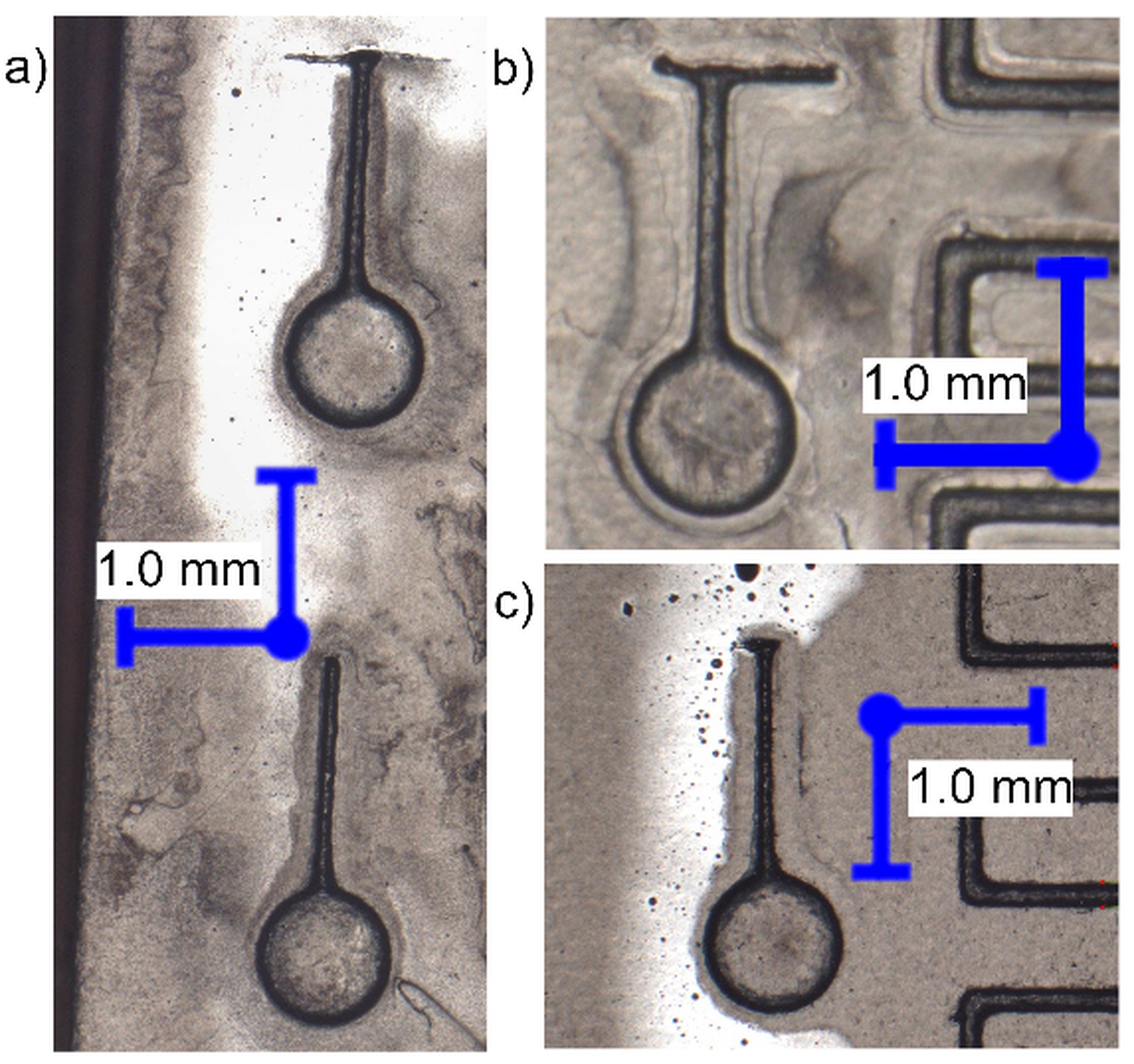
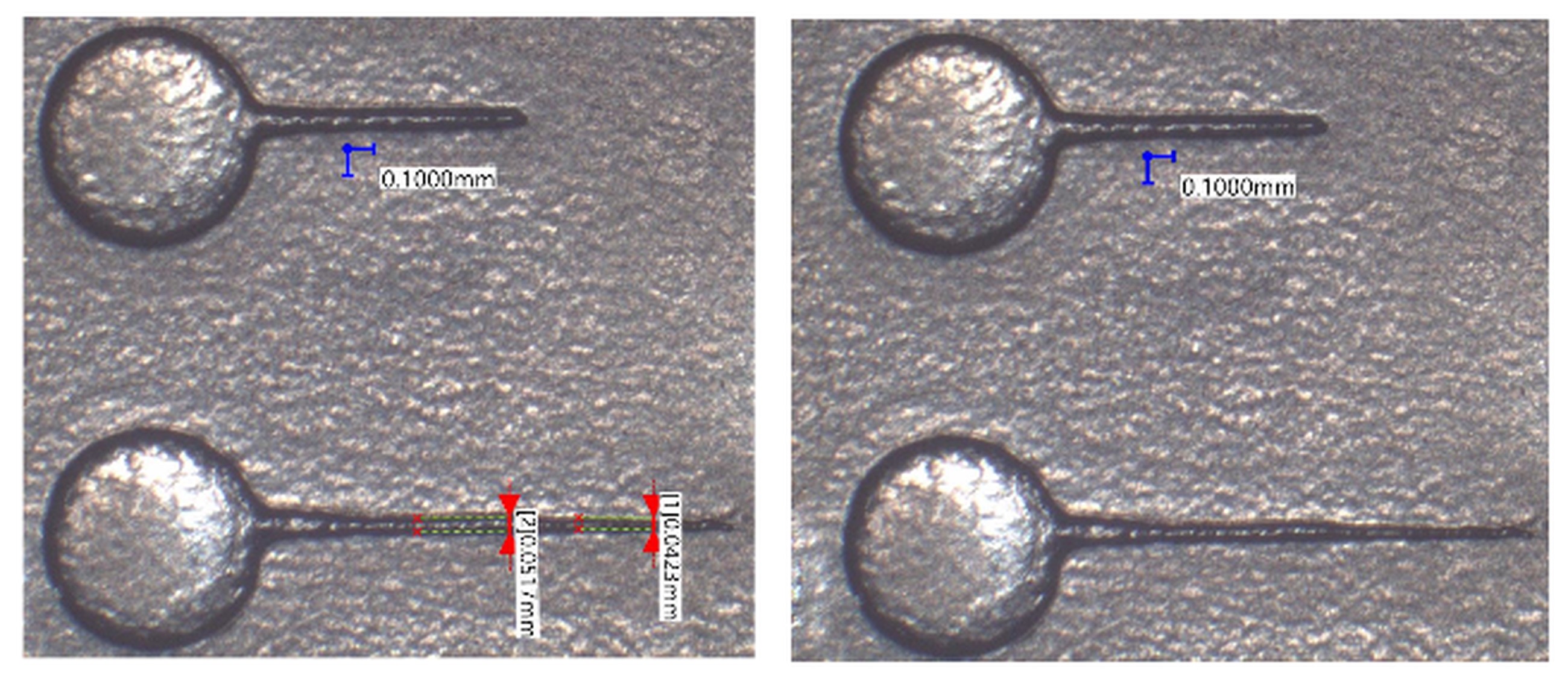
To complete the goals of this study, an LCD 3D printer was selected – Anycubic Photon Mono M5s (Shenzhen Anycubic Technology Co., Ltd., Shenzen, China) which offers an LCD screen with a resolution of 11520 per 5120 pixels. Additionally, the device utilizes ACF vat lining, for which adhesion forces are smaller than traditional FEP film. That, with the screen dimensions of 218 per 123 mm gives the single pixel size (theoretically the smallest printable feature) of approximately 19 per 24 µm. With that in mind, samples were designed to test the capabilities of manufacturing certain features desirable for molding MF devices. Several of the patterns selected are presented with important dimensions on Fig. 1. On each of the patterns presented here, the circular elements at the beginning of the channels have the same diameter of 0.8 mm and serve 2 purposes – to emulate the pump interface of MF device, and to anchor the delicate material forming the channel to the rest of the test sample during manufacturing process. Patterns a) and b) were designed to determine possibilities of forming 90° split patterns with decreasing channel cross-section.
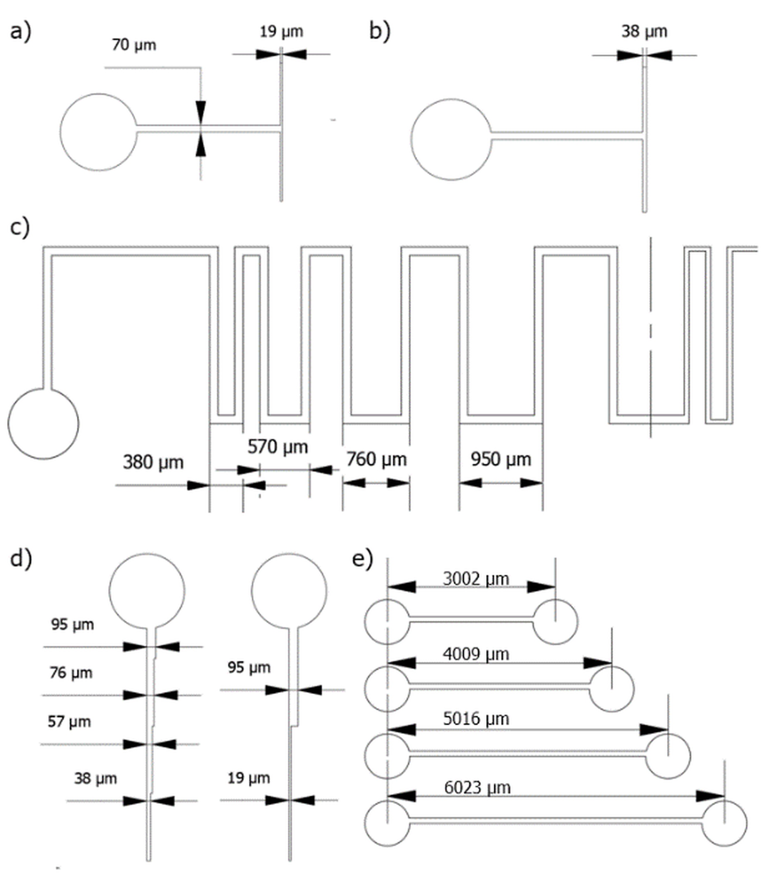
Fig. 1. Shapes of the dies designed for tests, with dimensions; a), b) channel split (90°); c) Zigzag pattern with increasing distance between direction changes; d) decreasing channel cross-section; e) channel length test. In the discussion section the patterns will be abbreviated by letters on the figure. (p1a, p1b, p1c… etc.)
Zigzag pattern (Fig. 1. c) was designed to determine whether the length of horizontal parts of the channel influences the printability and dimensions of the sample. The pattern continues with decreasing channel cross-section (after the dash-dot (-.) line on the drawing), but with decreased channel cross-section. Features shown on d) were designed to examine the influence of decreasing channel cross dimension done in small and large decrements. Pattern e) is to determine the influence of the channel’s length. Those patterns were fitted on 2 different test samples, both of which are shown in Fig. 2 (named sample types S1 and S2 respectively).
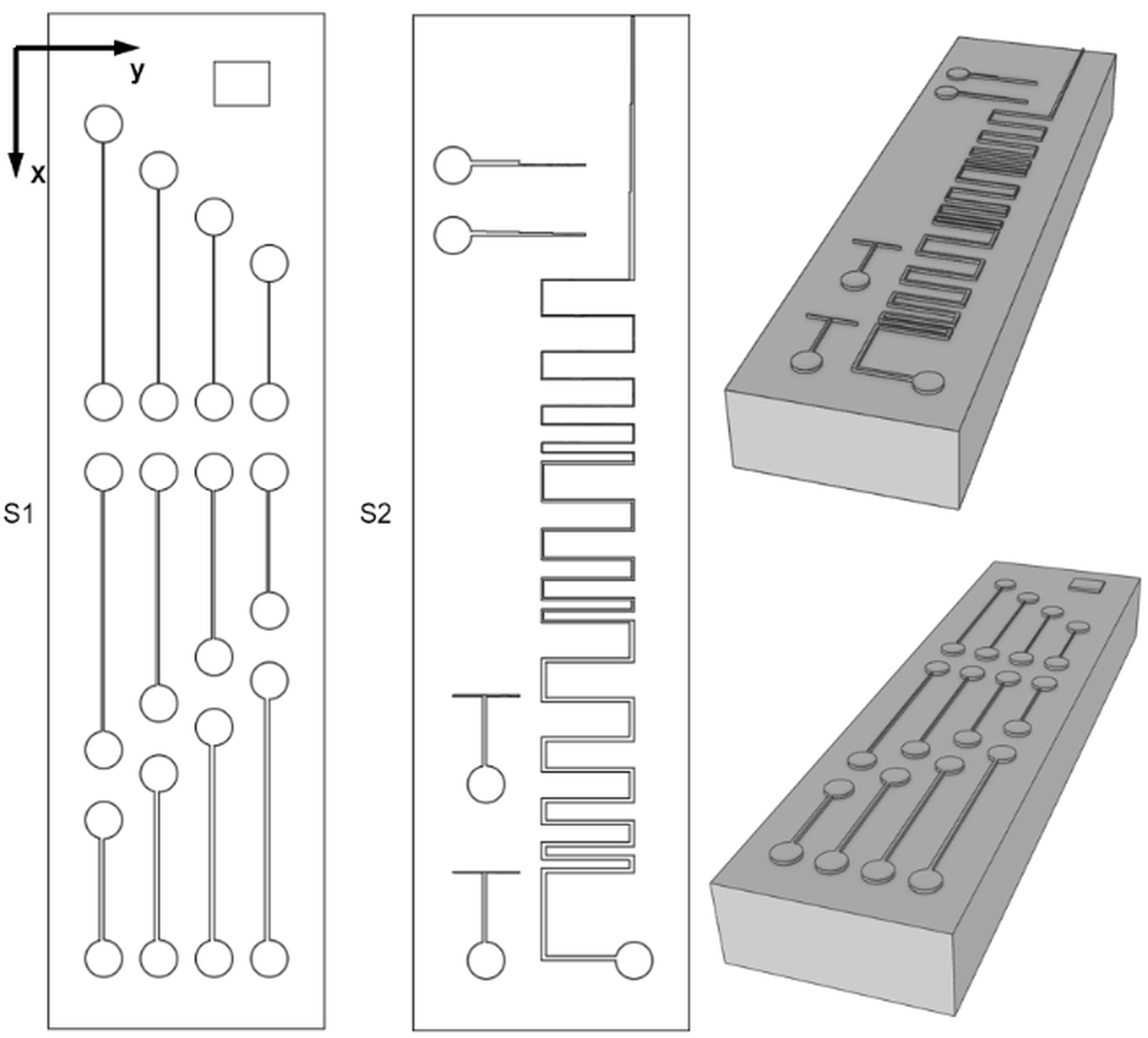
Fig. 2. Test sample types and their topology. The axes are marked to help address the patterns in the text
The 3D digital models of samples were created with Autodesk Inventor 2022 software and exported to stereolithography (.stl) file format. The overall dimensions of the sample’s supporting plate are 22.0x6.0x2.5 mm. By the authors’ experience, the thickness of 2.5 mm provides enough rigidity to prevent warping caused by shrinkage during the sample’s curing process. It is important to note, that due to the designed feature’s size, placement of each detail was calculated to fit the pixel mesh of the printer’s screen. With improper placement, the software that prepares input files for the printer will not reproduce the shapes properly. The software used to prepare beforementioned file was Anycubic Photon Workshop (APW). All of the programs prepared were inspected in APW. Fig. 3 shows part of the inspection screens, where the upper one maintains proper channel cross-dimensions, and the bottom one shows differences in light intensity (dimmed line) and channel thickness due to improper sample placement.
The material selected for manufacturing was Anycubic High-Speed Resin (Shenzhen Anycubic Technology Co., Ltd., Shenzen, China), as a material that was specifically designed for the selected printer’s model, offers good fluidity, and in initial tests displayed no noticeable shrinkage. The material in its original container was shaken manually for 2 minutes.

Fig. 3. Inspection screen of the APW slicing software. Upper picture shows properly placed and designed sample. Bottom side shows improperly placed sample
After that, the container was opened and unsealed, and placed in a vacuum chamber (VC2523A, vacuumchambers.eu, Bialystok, Poland) for degasification. The material was degasified until the negative pressure displayed on the chamber’s manometer reached -1 bar and no visible bubbles were present on the surface of the liquid pre-product (Fig. 4). Afterwards the prepared material was slowly poured into the machine’s resin vat to prevent mixing with air. The temperature of the resin was equalized with in-lab temperature (23 °C).
The principle of work of the machine is shown schematically on Fig. 5. The buildplate (1) submerges into the resin (3) placed in the vat (4) leaving a distance between the ACF (5) and manufactured part (2) equal to desired layer height.
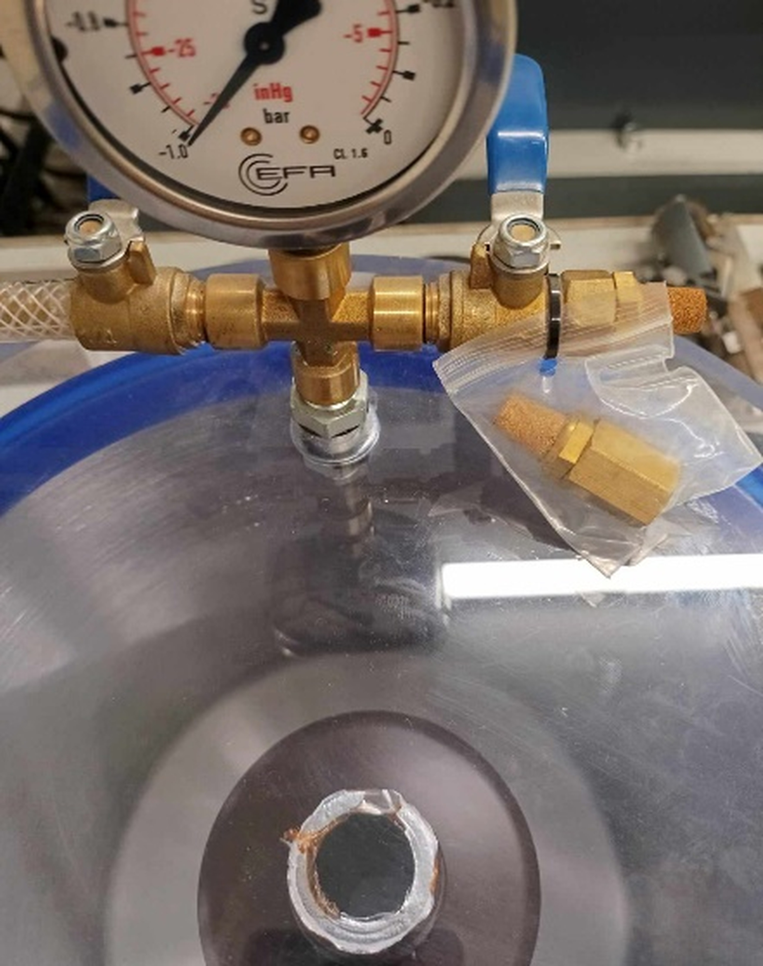
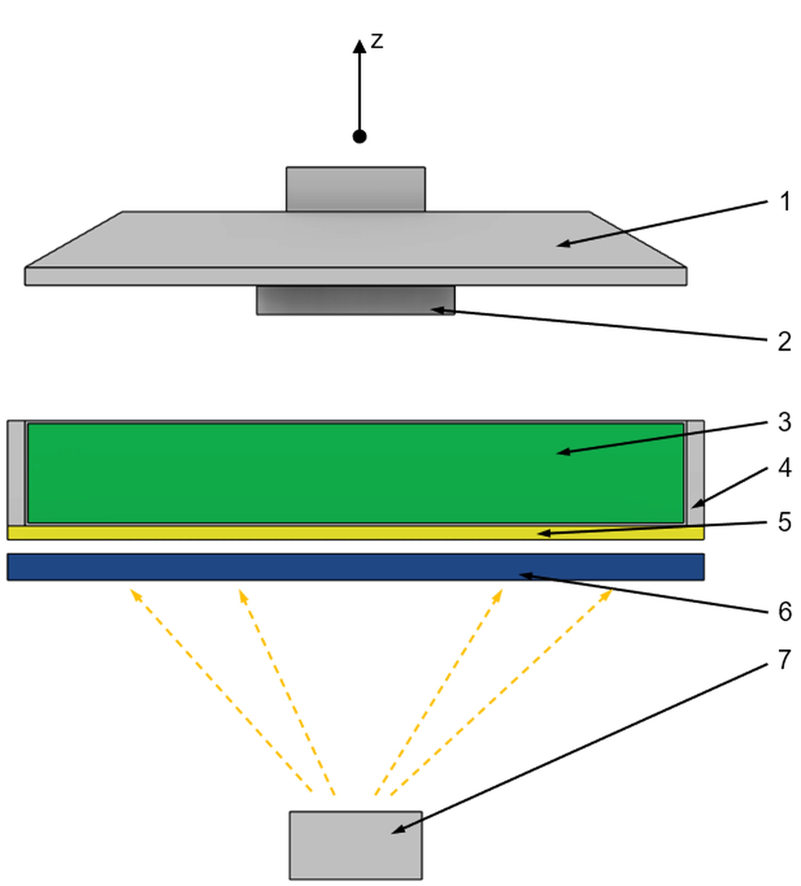
Fig. 5. Schematics of the 3D printing machine. 1 – Buildplate; 2 – Formed object; 3 – Liquid resin; 4 – Resin vat; 5 – Advanced composite film (ACF) lining; 6 – LCD screen; 7 – UV light source
Afterwards, a negative image of the layer is displayed on LCD screen (6) creating a mask, to cure the resin. The process is repeated until the whole object is formed. The samples were printed in groups of 6 samples (3 S1 samples and 3 S2 samples) with different process parameters for each group (Tab. 1). Multiple samples were printed, to observe how and if the imperfections and wear on ACF influences the sample quality.
Tab. 1
Selected non-constant parameters for different groups of samples
SG (Sample group n.) | 1 | 2 | 3 | 4 | 5 | 6 |
LT (Layer thickness), in mm | 0.1 | 0.02 | ||||
NET (Normal exposure time), in s | 1.5 | 0.9 | 1.5 | |||
BET (Bottom layer exposure time), in s | 4 | 7 | 4 | 7 | 7 | 7 |
AA (Antialiasing) | OFF | ON | ||||
In the table, the parameters used for the manufacturing process are presented. The parameters were decided on iteratively – after manufacturing each group of samples and examining them, a new set of parameters was selected, to improve on the imperfections observed. Other constant parameters include Z-lift height (on the Z axis after each layer, in mm): 6; Z-lift speed (in mm/s): 4; the number of bottom layers (with higher exposure time presented in the table): 3.
After the manufacturing process, the samples were carefully removed from the buildplate with a scraper, cleaned with isopropyl alcohol and exposed to UV light for 15 minutes. Between processes, the bottom of the resin vat was cleaned from potential debris, by turning on the printer’s light source for 30 seconds and removing the hardened layer with a plastic spatula.
For observations and analysis, the Keyence VHX-7000 optical microscope (Keyence Corporation, Osaka, Japan) was utilized. The apparatus offers magnification up to 2000 times and enables on-screen live dimensional measurements of the observed image.
The samples and shapes produced were then assessed in terms of:
Ability to reproduce theoretical shape,
Changes in theoretical dimensions caused by shrinkage and overmolding/curing,
Process parameters that led to the best result,
Influence of other non-controllable factors on the process and the sample.
Calibration of the on screen measurement function of the microscope was checked by measuring dimension of a calibration sample with known dimensions. All of the observations with dimensions measurements were done with full central top light, if not stated otherwise in the text.
Results And Discussion
Macroscopic photographs of selected samples are presented in Fig. 6. The blue scale on each photo represents a distance of 1.0 mm.
In general, the first observations can be made from the photographs:
There are visible differences in light reflectivity of the surface.
Some of the debris and defects can be observed, with different intensity across specimens.
The features that were fully formed differ, even among specimens manufactured with the same process parameters.
Some of the channels are not straight where they are supposed to be.
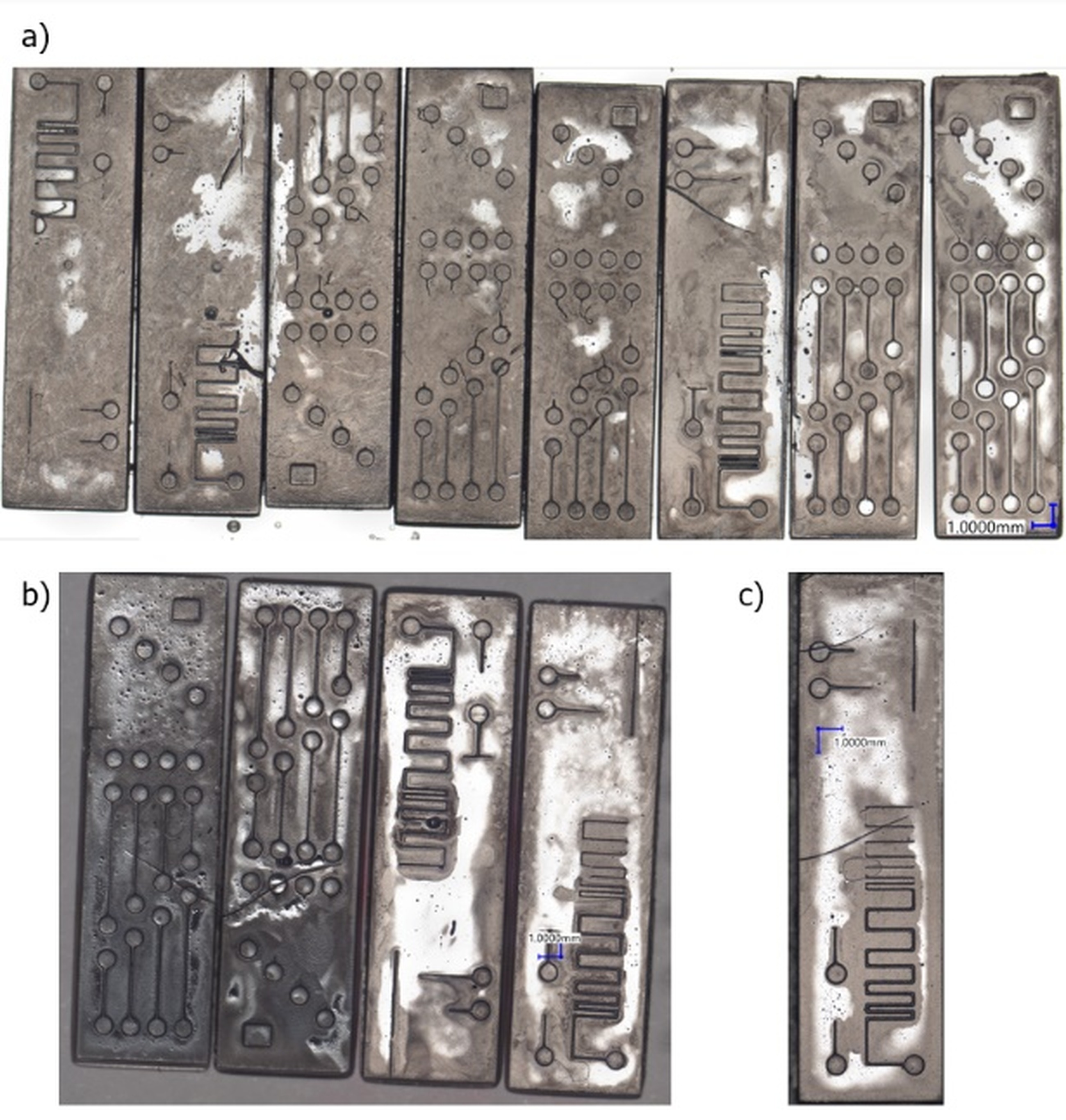
Fig. 6. Macroscopic photographs of selected samples. Process parameters: a) SG (s ample group number) 1 and 2; b) SG 5 c) SG 6. The blue scale on each drawing represent dimension of 1 mm
It is possible to name factors leading to such defects. The glossiness of random areas, not visible to the naked eye can be caused by the distribution of particles within the resin, which is in its form – a colloidal liquid. Despite proper mixing procedure, factors such as time in the vat, the flow of the resin during buildplate movements, etc. influence beforementioned distribution. On some specimens minor cracks are visible. The cracks are caused by the extraction process. When the samples were detached from the buildplate, due to the high adhesion of the specimen to the plate, a larger force had to be applied, sporadically causing faint cracks. Lower adhesion was achieved with BET=4 s, but due to delamination issues, that value was increased to 7 for other sets of specimens. The debris and small irregularities on the specimen surface are caused by detached, misprinted parts of small features, and by imperfections on the surface of ECF.
To understand measured values, a 3D depth composition image was created (Fig. 7).
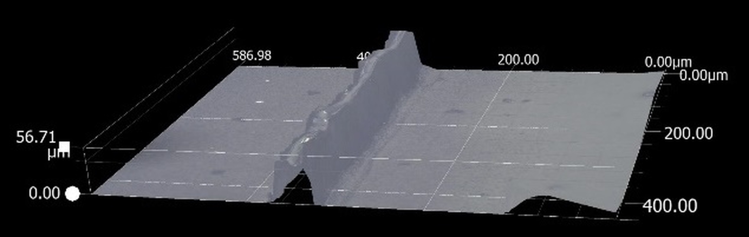
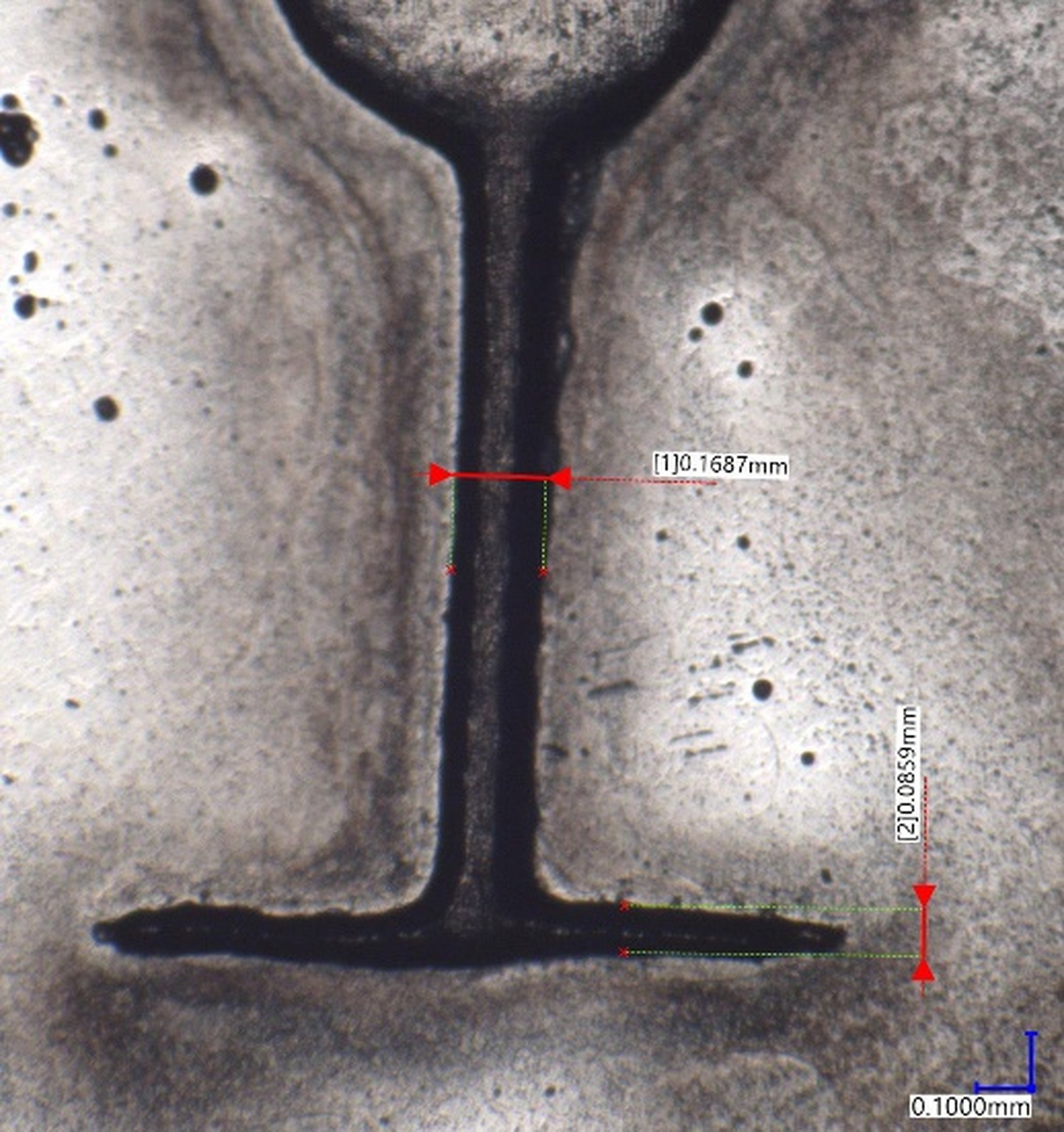
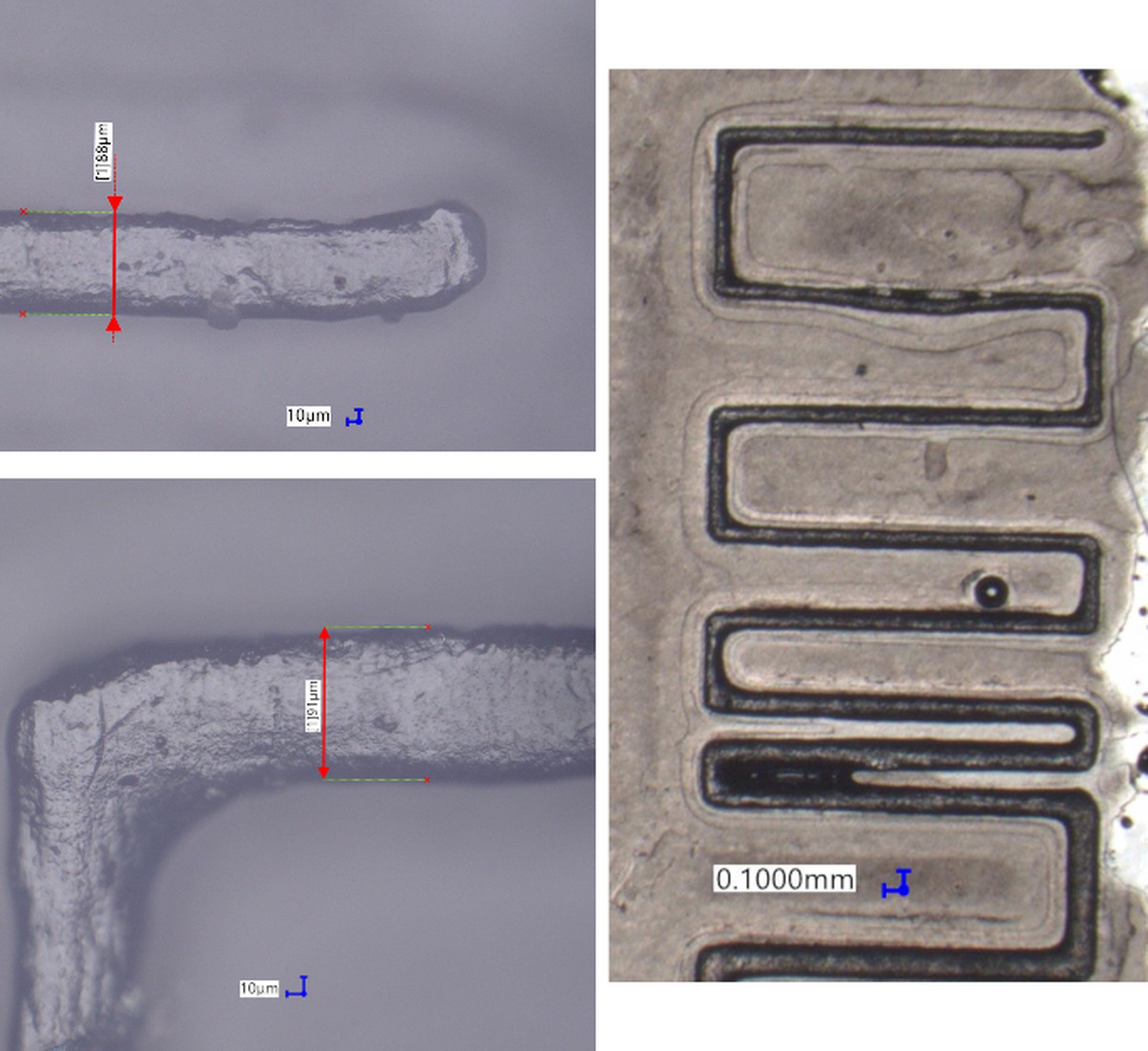
Figure 8 provides more detailed information about the depth composition image. Images a) and b) were taken with a different lens than c), to capture smaller area more accurately, thus the difference in sample coloration. A small rounded area near the bottom of the protrusion is present (Fig. 8. b), which is not distinguishable in the photograph with default lens and illumination (Fig. 8. c), causing an illusory increase in the measured feature thickness. The pattern presented is PLA, with a theoretical (from the model) path thickness of 70 µm. On the photograph a), the blurred area represents the uppermost surface of the protrusion. The tapered cross-section visible in Fig. 7, and before mentioned rounding at the bottom creates the 59 – 70 – 82 µm difference in the reading between observations.
Another observation taken with high magnification lens was for examining the top surface of the protrusion. Figure 9 displays surface of the path from pattern p1e with model thickness of 48 µm. The measured thickness is 40 µm which coincides with observations from depth composition analysis (rounding and tapered surface are out of focus on this photograph). The surface is composed of small grains, with visible “stretch marks” colinear with the protrusion. The right side image also shows small oval dents, the largest being 4 µm in diameter. Small changes in the channel height are also visible on both depth composition and top surface images, not exceeding 10 µm, on the features that were successfully formed. Those changes could be caused by either shrinkage during the curing process or by micro-delamination when, during manufacturing, the layer is being separated from the ACF.
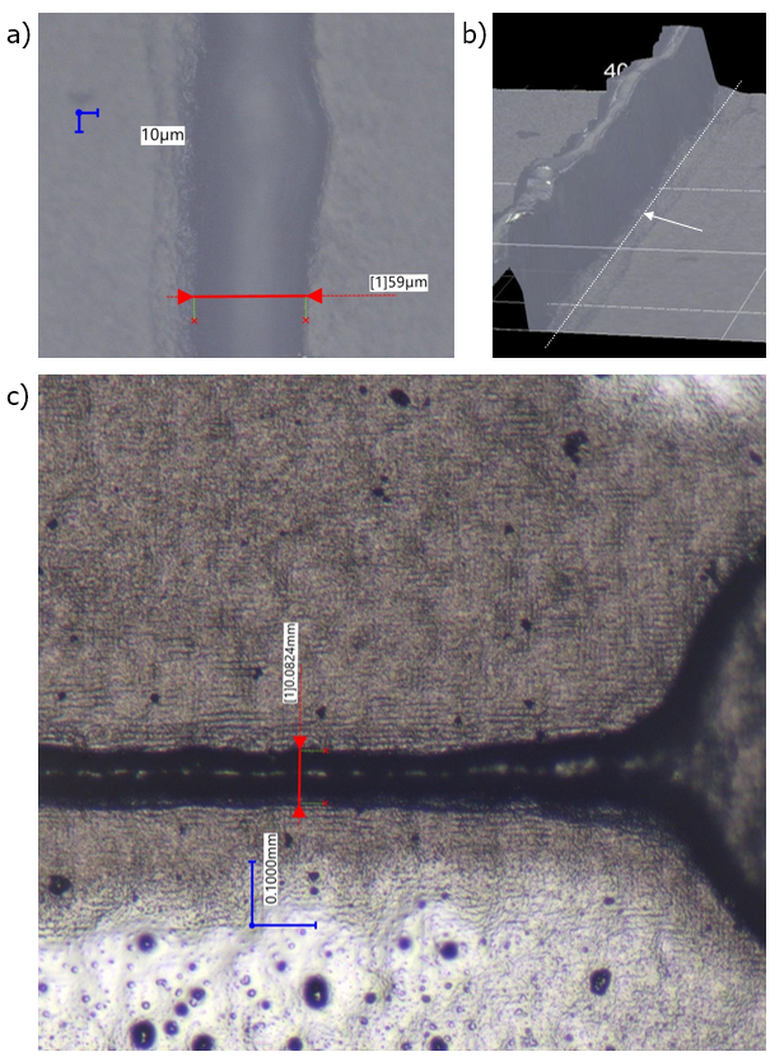
Fig. 8. Localization of performed depth composition; a) channel thickness with microscope lens focused on the lowest surface; b) Observed rounding at the foot of the channel, marked by the arrow; c) measurement in the same location (pattern p1 a) with default (central) illumination and magnification
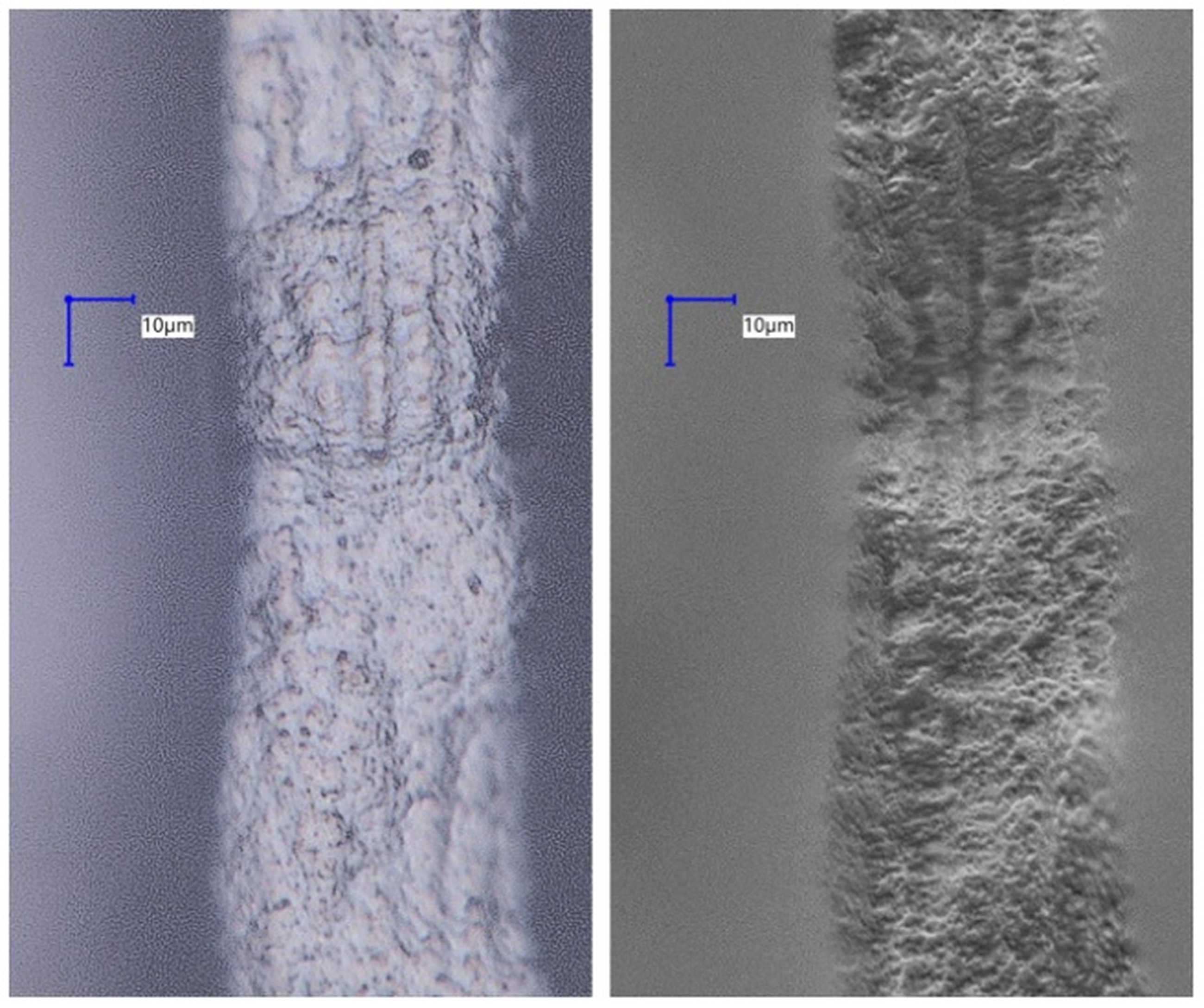
Fig. 9. Top surface of the protrusion of pattern p1e, with LH=0.02 mm. Both pictures show the same area with different digital image enhancements, to make the microscopic features more readable. The scale represents 10 µm
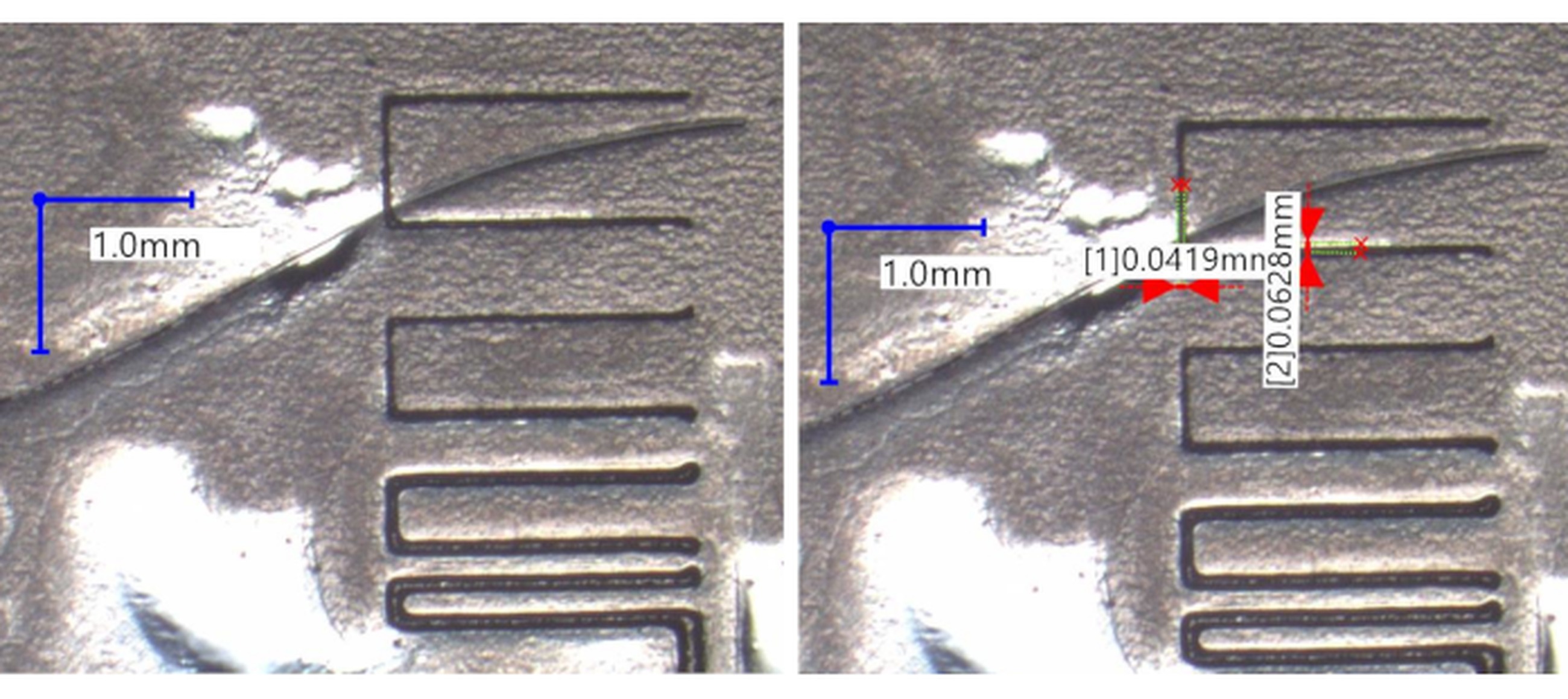
The only successful reproduction of shape p1b was achieved for SG 5. However, in this case, the structure was significantly overexposed, as visible on thickness measurements (Fig. 10): 169 µm vs theoretical 72 µm, and for the 90° split: 86 µm vs 38 µm. The thinner line also deviates from its straight theoretical path, presumably due to delamination. The mentioned result, along with the thinning of the line towards its end leads to the conclusion that the difficulty in reproducing the shape is caused by the lack of proper anchoring of such a delicate feature.
To test this conclusion, a sample within the same setup (the only difference being NET=0.9 s) was manufactured and is shown in the photograph (Fig. 11). In this case, the splitting structures are manufactured without loose ends, and no delamination is observed.
A different sample from SG 5 displays leftovers from the delaminated (perpendicular to the circular interface) part of the channel (Fig. 12. a), and the same thickness of the first channel part as the previously discussed one (169 µm). Fig. 12 b shows a properly formed perpendicular part on the right side of the photograph, but within SG 6 parameters, such a feature is also overmolded (thickness of 93 µm vs theoretical 38 µm). The initial part of the channel was correctly produced on every sample from SG 3, 4 and 6 with measured cross-sectional dimension within a range of 80-84 µm.
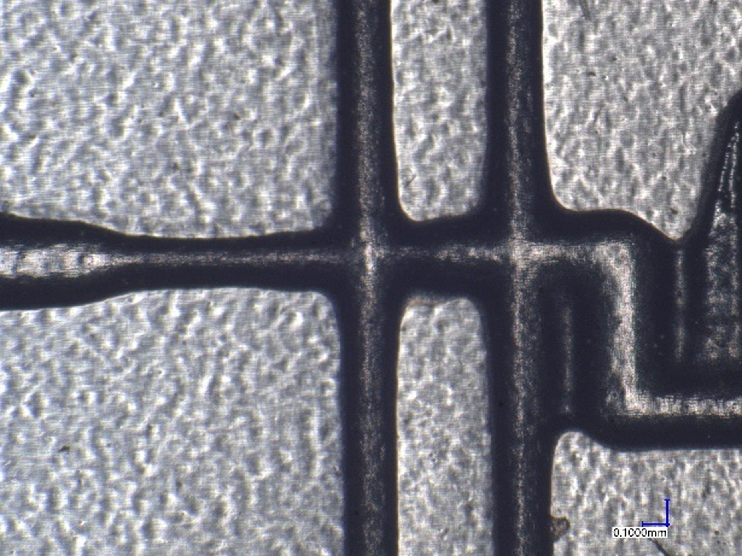
Fig. 11. 90° split manufactured as an additional test, but with a different shape (without loose path ends)
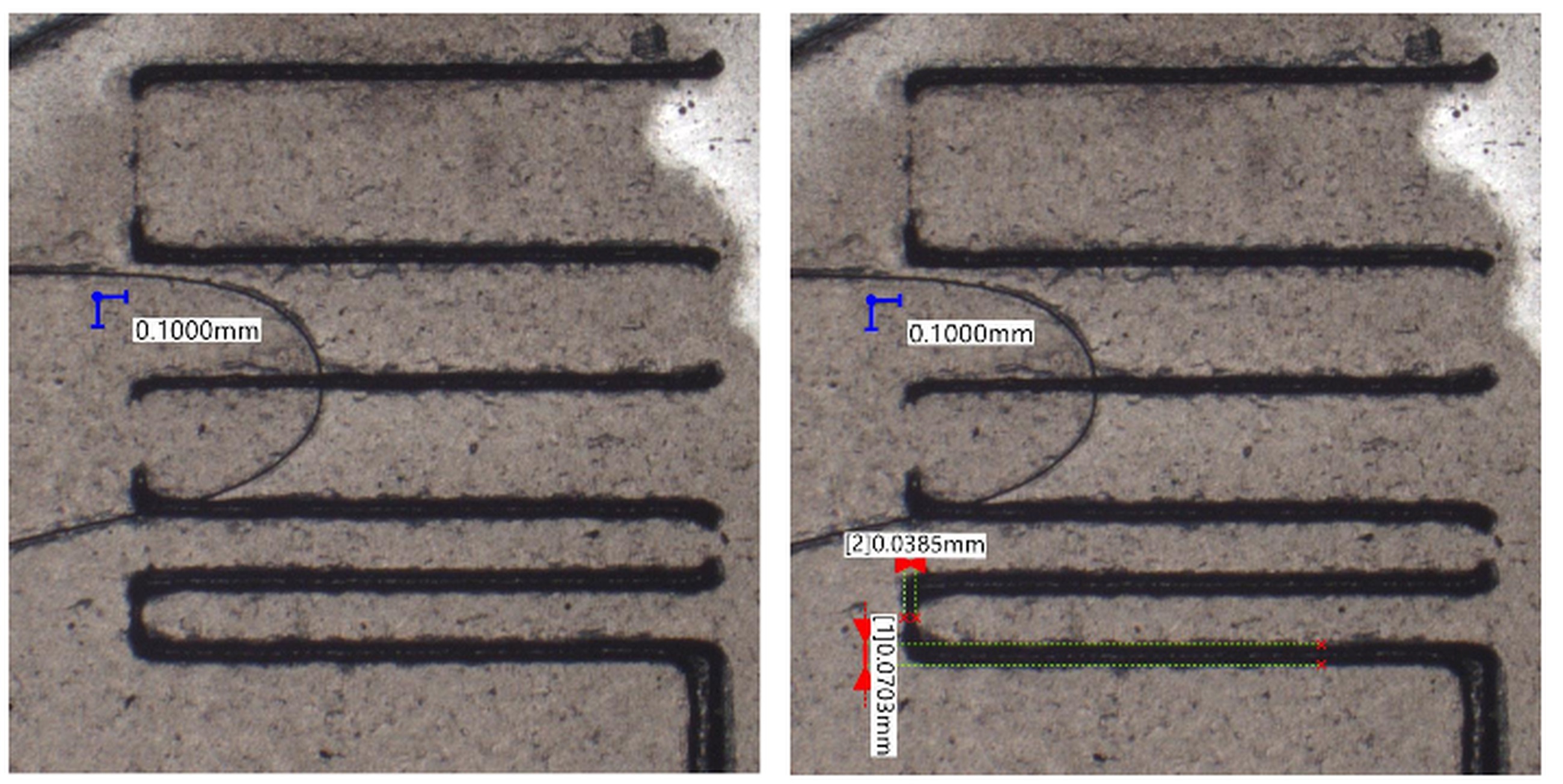
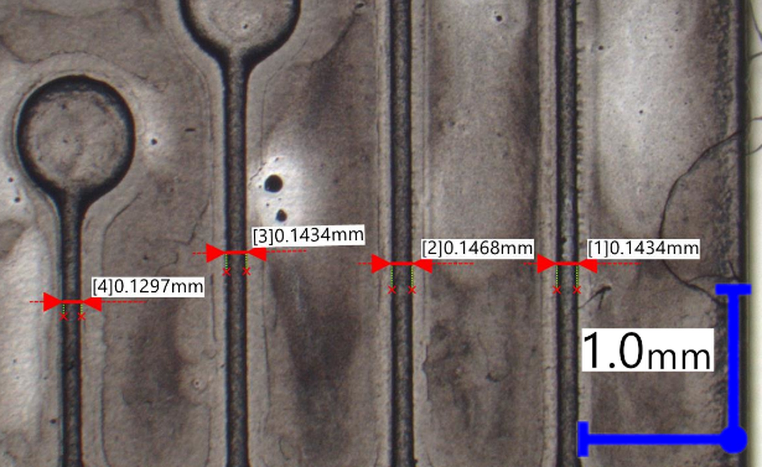
The shape of pattern p1c was correctly reproduced within every sample group on its first iteration (at a modelled thickness of the lines being 95 for the y axis part, and 96 µm for x). The second iteration of the pattern, with a line thickness of 57 in y and 48 µm in x was shaped correctly for every pattern within y axis, but with some damage present within x-channel. On every sample, some rounding at the edges of the top view is present, which is expected behavior. Significant thickening of the paths is observed for SG1 and SG2, at the part where the path along x axis is the shortest (Fig. 13). Such effect is observed to be standard behavior in those groups, and can be additionally explained by the material being trapped between the lines, thus being overly cured within the area (as overmolding between paths is also visible on the figure). The overmolding effect is not observable for SG4.
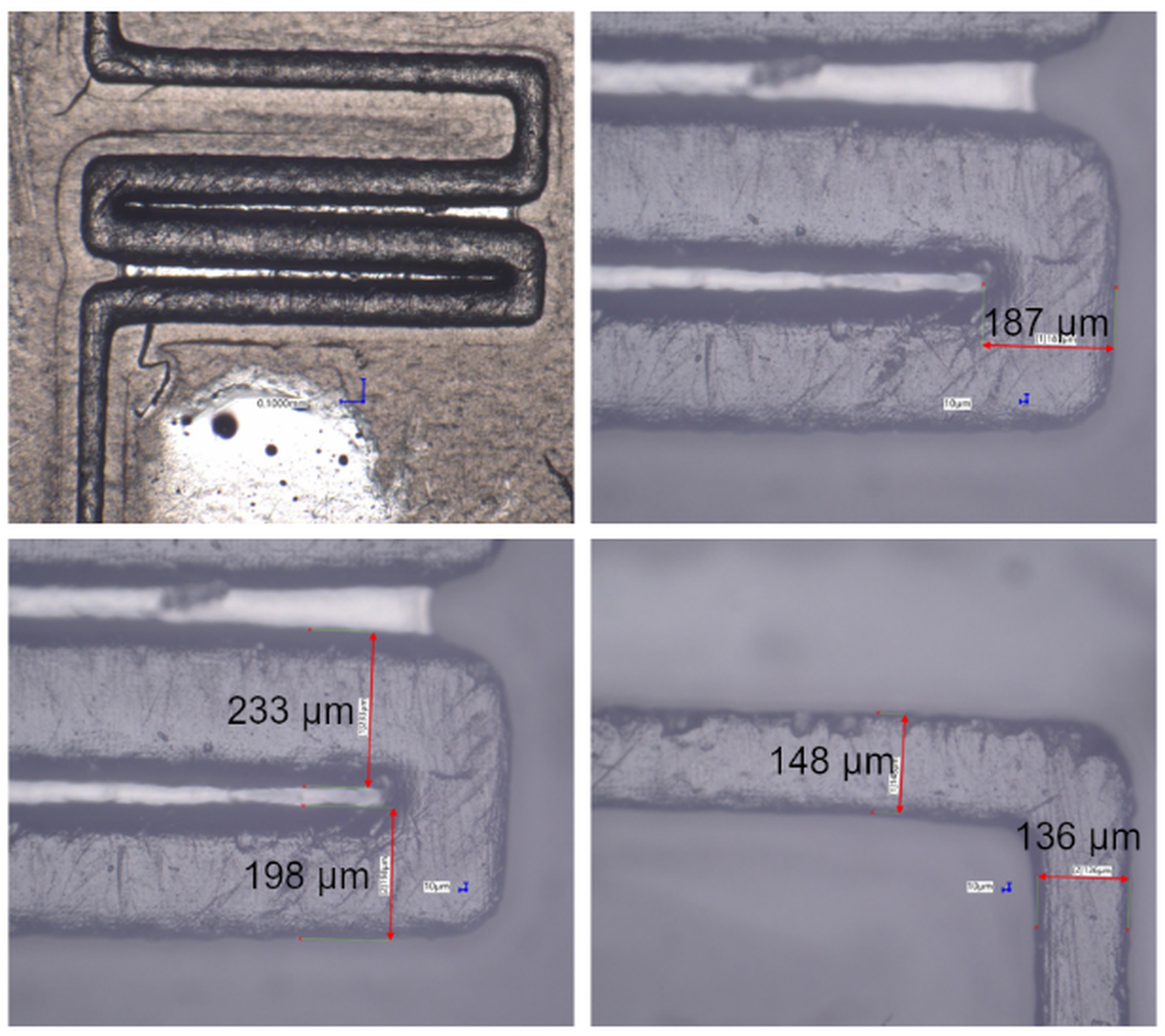
On the areas of the pattern where distances between y-axis lines are larger, the thickness of the paths tends to be smaller, with thickness between the range 130-150 µm. To a smaller extent, overcured material is also present in SG2 at the beginning of the second iteration. The channel there is also thicker than modelled (Fig. 14).
In SG4 on the second iteration of the pattern, the cross-section of the line is smaller than modelled, and fits within a range of 40-50 µm (x) and 55-65 µm (y) (Fig. 15). Consistently, for every sample group, paths along x-axis tend to be improperly formed on the side of the specimen’s edge. Correspondent paths on the other side of the pattern are at least partially formed or fully formed. SG4 thinning can be expected due to its smallest NET.
An interesting effect can be observed on a sample from SG6 (Fig. 16). As presented in the figure, a thinner than expected (modelled 48 µm) x connector can be formed if the lines are closer together. Otherwise, structures along x are not repeatable. No overmolding is observed on the y-axis.
Pattern p1d, designed to test the possibility of forming gradually decreasing channel cross-section dimension and quickly changing cross-section dimension didn’t show success in the latter part, but for the former, the shape was reproduced for SG4, 6 and 7. In SG 1 and 2, the protrusion delaminates fully at the section where the dimension gets smaller, or in one case partially as visible in Fig. 17. Consistently in this SG, the first part’s thickness is increased and measures between 120 and 130 µm instead of ideal 95.
SG4 achieved the best results, with a fully formed channel (despite NET=0.9 s) and a gradual decrease in thickness, with the smallest cross-section dimension measuring 30 µm at the end. The cross-section of these was slightly under the expected dimensions, measuring 52 vs 57 and 42 vs 38 µm (measured vs theoretical, Fig. 18). Dimension of 42 µm is considered under-cured because of the previous observation of the tapered edges and rounding at the foot of the structure.
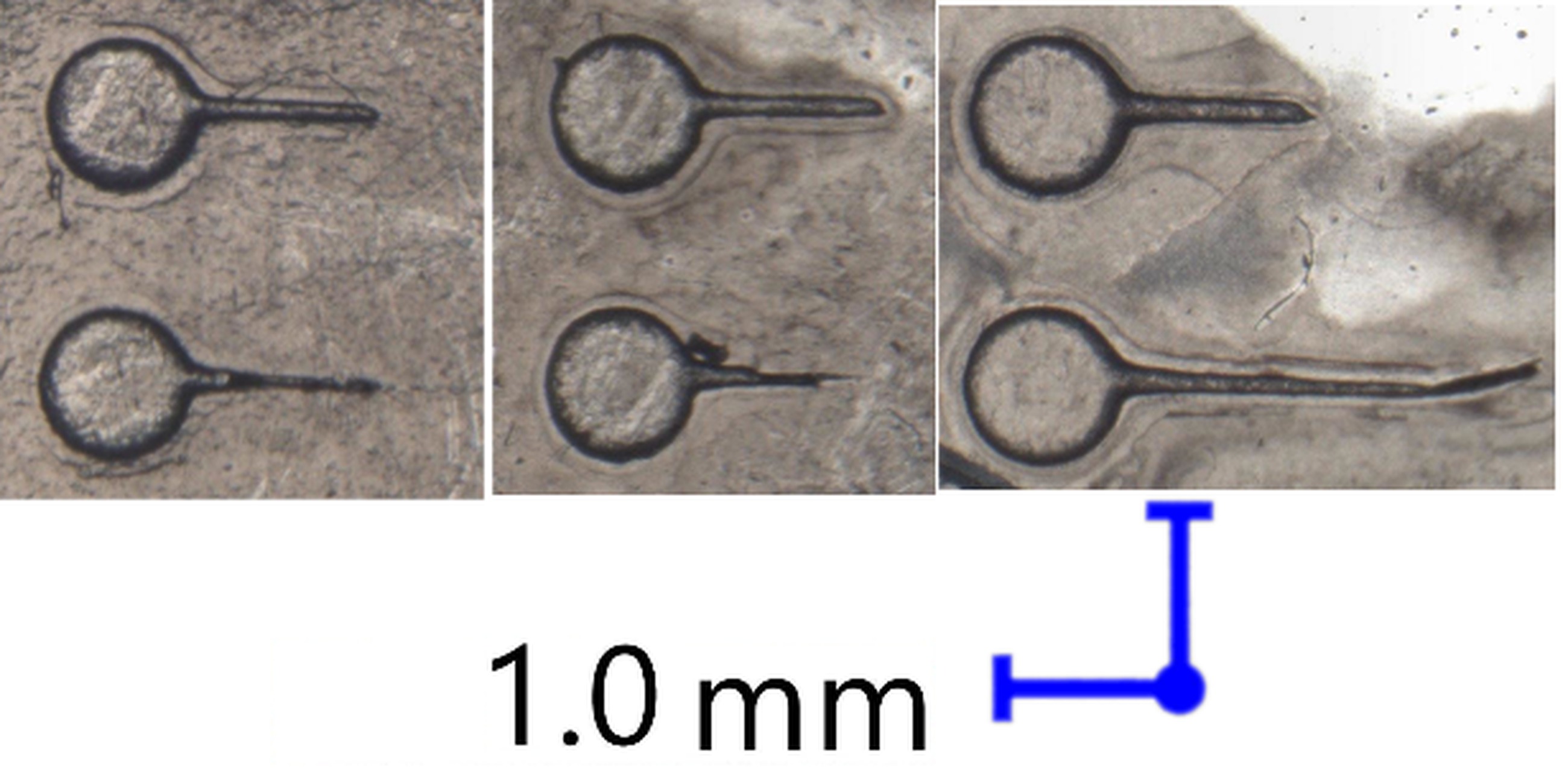
The last pattern – p1e, with straight continuous channels – was correctly manufactured within the full range of protrusion lengths of model thicknesses of 96 and 48 µm. 24 µm channels were never fully manufactured due to delamination issues. Similarly to previous patterns, samples from SG1 and 2 were overcured, with their thickness ranging from 130 µm (shortest channel, 96 µm thickness by model) to 143-147 µm for the longer channels (same model thickness) (Fig. 19).
Ideal channel thickness (for modelled 48 µm) was observed in SG5 and 6, ranging between 62 and 65 µm measured.
Conclusions
Printing multiple samples at the same time is not recommended due to the potential increase in the amount of delaminated debris, affecting other prints
Parameters from SG1 and 2 can be used to consistently form structures with dimensions >80 µm, but overcuring has to be accounted for in the model.
Most of the improperly formed structures presented in the study are damaged due to delamination during layer changes. Since that’s the largest contributor to the failure rate, in future study it is necessary to find methods decreasing adhesion forces between the vat and freshly formed layers, and to decrease the stress generated by the separation.
Shrinkage of the material does not play a role in the described manufacturing process, nevertheless it has to be accounted for in angled transitions, as the structures exhibit roundings on the edges.
Features at the smallest possible scale (in the case of this study pixel size 19x24 µm), cannot be manufactured properly for larger channel lengths, but can be used for thinning thicker channels locally on a short distance (smaller than 200 µm).
Under-cured features were observed in SG3 and 4, whereas over-curing was observed in SG1 and 2. In the former – due to the smallest NET (0.9 s), and in the latter because of high LT (0.1 mm). Some overcured material was also found in the areas between protrusions, if they were small enough and encapsulated (380 µm channel x-distance in pattern p1c).
To form the thinnest channels, proper anchoring to a larger structure is required.